

[129], with the latter shifting to long wavelengths with the increasing aspect ratio,
as predicted by Link et al. [322] Nanowires of bismuth with a diameter of 1 nm
have been obtained by filling SWNTs during arc vaporization as well as by a solution method [323]. Interestingly, by employing the anodic aluminum oxide (AAO)
templates and organometallic chemical vapor deposition (MOCVD), nickel nanowires of 4 nm diameter have been produced inside the carbon nanotubes [324].
However, the diameter of the AAO templates dictates the diameter of the nanowires, making it difficult to tune the nanowire diameter down to 1 nm. SWNTs
with a narrow size distribution seem to have an advantage as ideal templates
[323, 325].
Solution–Liquid–Solid Process Buhro and coworkers [276], have developed a low
temperature solution–liquid–solid (SLS) method for the synthesis of highly crystalline nanowires of III–V semiconductors [276, 327]. In a typical procedure, a
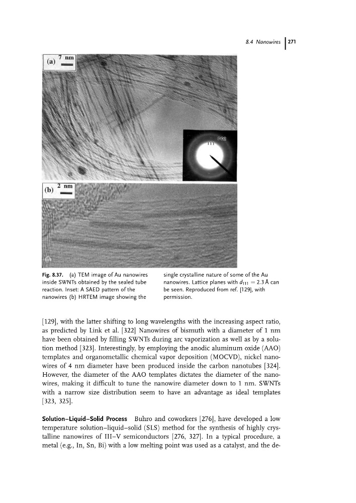
metal (e.g., In, Sn, Bi) with a low melting point was used as a catalyst, and the deFig. 8.37. (a) TEM image of Au nanowires
inside SWNTs obtained by the sealed tube
reaction. Inset: A SAED pattern of the
nanowires (b) HRTEM image showing the
single crystalline nature of some of the Au
nanowires. Lattice planes with d 111 ¼ 2:3 A ˚ can
be seen. Reproduced from ref. [129], with
permission.
8.4 Nanowires 271
as predicted by Link et al. [322] Nanowires of bismuth with a diameter of 1 nm
have been obtained by filling SWNTs during arc vaporization as well as by a solution method [323]. Interestingly, by employing the anodic aluminum oxide (AAO)
templates and organometallic chemical vapor deposition (MOCVD), nickel nanowires of 4 nm diameter have been produced inside the carbon nanotubes [324].
However, the diameter of the AAO templates dictates the diameter of the nanowires, making it difficult to tune the nanowire diameter down to 1 nm. SWNTs
with a narrow size distribution seem to have an advantage as ideal templates
[323, 325].
Solution–Liquid–Solid Process Buhro and coworkers [276], have developed a low
temperature solution–liquid–solid (SLS) method for the synthesis of highly crystalline nanowires of III–V semiconductors [276, 327]. In a typical procedure, a
metal (e.g., In, Sn, Bi) with a low melting point was used as a catalyst, and the deFig. 8.37. (a) TEM image of Au nanowires
inside SWNTs obtained by the sealed tube
reaction. Inset: A SAED pattern of the
nanowires (b) HRTEM image showing the
single crystalline nature of some of the Au
nanowires. Lattice planes with d 111 ¼ 2:3 A ˚ can
be seen. Reproduced from ref. [129], with
permission.
8.4 Nanowires 271