

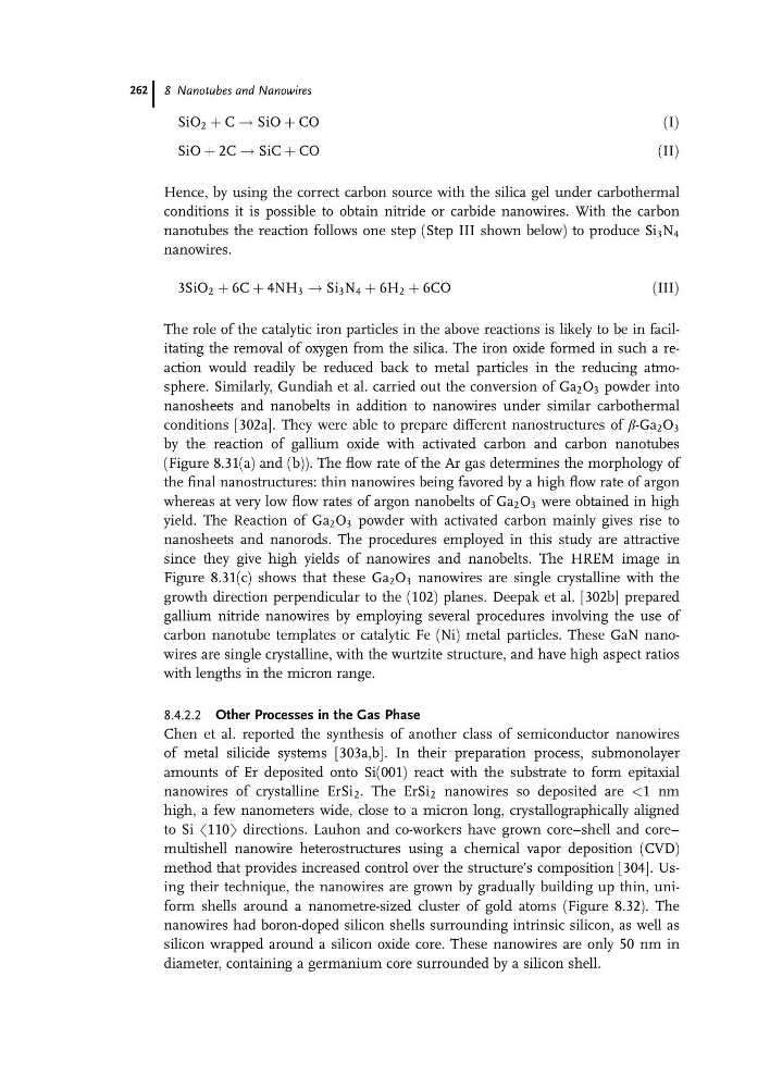
SiO 2 þ C ! SiO þ CO
ðIÞ
SiO þ 2C ! SiC þ CO
ðIIÞ
Hence, by using the correct carbon source with the silica gel under carbothermal
conditions it is possible to obtain nitride or carbide nanowires. With the carbon
nanotubes the reaction follows one step (Step III shown below) to produce Si 3 N 4
nanowires.
3SiO 2 þ 6C þ 4NH 3 ! Si 3 N 4 þ 6H 2 þ 6CO
ðIIIÞ
The role of the catalytic iron particles in the above reactions is likely to be in facilitating the removal of oxygen from the silica. The iron oxide formed in such a reaction would readily be reduced back to metal particles in the reducing atmosphere. Similarly, Gundiah et al. carried out the conversion of Ga 2 O 3 powder into
nanosheets and nanobelts in addition to nanowires under similar carbothermal
conditions [302a]. They were able to prepare different nanostructures of b-Ga 2 O 3
by the reaction of gallium oxide with activated carbon and carbon nanotubes
(Figure 8.31(a) and (b)). The flow rate of the Ar gas determines the morphology of
the final nanostructures: thin nanowires being favored by a high flow rate of argon
whereas at very low flow rates of argon nanobelts of Ga 2 O 3 were obtained in high
yield. The Reaction of Ga 2 O 3 powder with activated carbon mainly gives rise to
nanosheets and nanorods. The procedures employed in this study are attractive
since they give high yields of nanowires and nanobelts. The HREM image in
Figure 8.31(c) shows that these Ga 2 O 3 nanowires are single crystalline with the
growth direction perpendicular to the (102) planes. Deepak et al. [302b] prepared
gallium nitride nanowires by employing several procedures involving the use of
carbon nanotube templates or catalytic Fe (Ni) metal particles. These GaN nanowires are single crystalline, with the wurtzite structure, and have high aspect ratios
with lengths in the micron range.
8.4.2.2 Other Processes in the Gas Phase
Chen et al. reported the synthesis of another class of semiconductor nanowires
of metal silicide systems [303a,b]. In their preparation process, submonolayer
amounts of Er deposited onto Si(001) react with the substrate to form epitaxial
nanowires of crystalline ErSi 2 . The ErSi 2 nanowires so deposited are <1 nm
high, a few nanometers wide, close to a micron long, crystallographically aligned
to Si h110i directions. Lauhon and co-workers have grown core–shell and core–
multishell nanowire heterostructures using a chemical vapor deposition (CVD)
method that provides increased control over the structure’s composition [304]. Using their technique, the nanowires are grown by gradually building up thin, uniform shells around a nanometre-sized cluster of gold atoms (Figure 8.32). The
nanowires had boron-doped silicon shells surrounding intrinsic silicon, as well as
silicon wrapped around a silicon oxide core. These nanowires are only 50 nm in
diameter, containing a germanium core surrounded by a silicon shell.
8 Nanotubes and Nanowires
262
ðIÞ
SiO þ 2C ! SiC þ CO
ðIIÞ
Hence, by using the correct carbon source with the silica gel under carbothermal
conditions it is possible to obtain nitride or carbide nanowires. With the carbon
nanotubes the reaction follows one step (Step III shown below) to produce Si 3 N 4
nanowires.
3SiO 2 þ 6C þ 4NH 3 ! Si 3 N 4 þ 6H 2 þ 6CO
ðIIIÞ
The role of the catalytic iron particles in the above reactions is likely to be in facilitating the removal of oxygen from the silica. The iron oxide formed in such a reaction would readily be reduced back to metal particles in the reducing atmosphere. Similarly, Gundiah et al. carried out the conversion of Ga 2 O 3 powder into
nanosheets and nanobelts in addition to nanowires under similar carbothermal
conditions [302a]. They were able to prepare different nanostructures of b-Ga 2 O 3
by the reaction of gallium oxide with activated carbon and carbon nanotubes
(Figure 8.31(a) and (b)). The flow rate of the Ar gas determines the morphology of
the final nanostructures: thin nanowires being favored by a high flow rate of argon
whereas at very low flow rates of argon nanobelts of Ga 2 O 3 were obtained in high
yield. The Reaction of Ga 2 O 3 powder with activated carbon mainly gives rise to
nanosheets and nanorods. The procedures employed in this study are attractive
since they give high yields of nanowires and nanobelts. The HREM image in
Figure 8.31(c) shows that these Ga 2 O 3 nanowires are single crystalline with the
growth direction perpendicular to the (102) planes. Deepak et al. [302b] prepared
gallium nitride nanowires by employing several procedures involving the use of
carbon nanotube templates or catalytic Fe (Ni) metal particles. These GaN nanowires are single crystalline, with the wurtzite structure, and have high aspect ratios
with lengths in the micron range.
8.4.2.2 Other Processes in the Gas Phase
Chen et al. reported the synthesis of another class of semiconductor nanowires
of metal silicide systems [303a,b]. In their preparation process, submonolayer
amounts of Er deposited onto Si(001) react with the substrate to form epitaxial
nanowires of crystalline ErSi 2 . The ErSi 2 nanowires so deposited are <1 nm
high, a few nanometers wide, close to a micron long, crystallographically aligned
to Si h110i directions. Lauhon and co-workers have grown core–shell and core–
multishell nanowire heterostructures using a chemical vapor deposition (CVD)
method that provides increased control over the structure’s composition [304]. Using their technique, the nanowires are grown by gradually building up thin, uniform shells around a nanometre-sized cluster of gold atoms (Figure 8.32). The
nanowires had boron-doped silicon shells surrounding intrinsic silicon, as well as
silicon wrapped around a silicon oxide core. These nanowires are only 50 nm in
diameter, containing a germanium core surrounded by a silicon shell.
8 Nanotubes and Nanowires
262