

244
6 Photodetection Devices
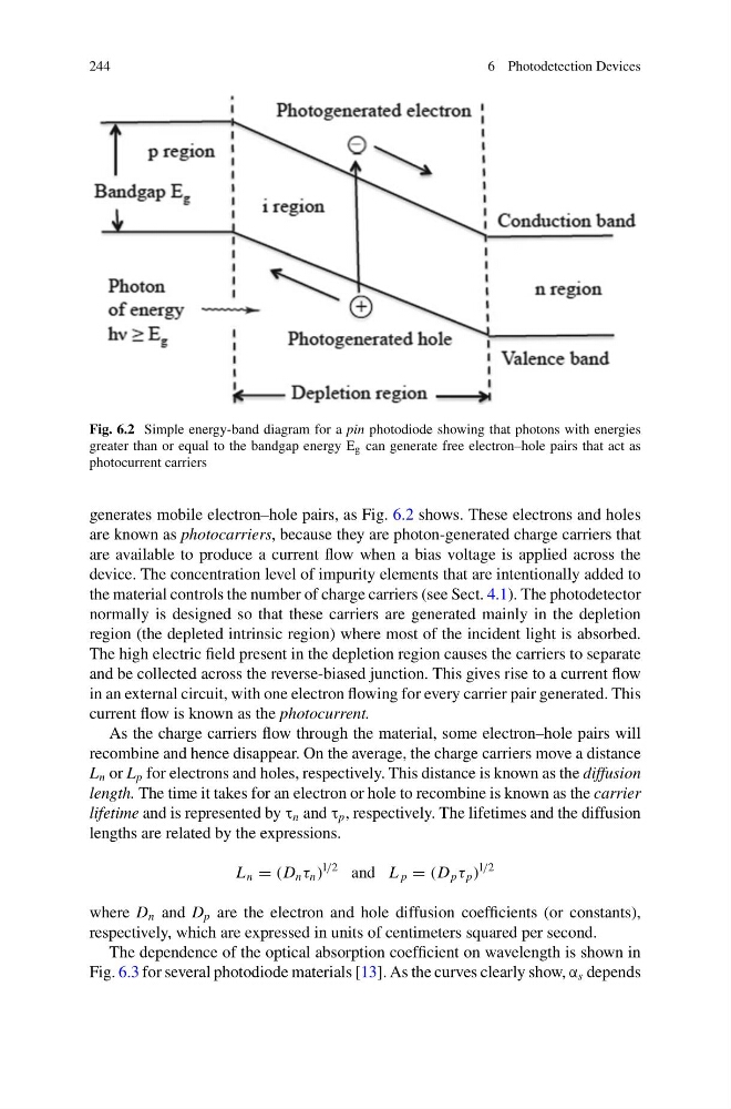
Fig. 6.2 Simple energy-band diagram for a pin photodiode showing that photons with energies
greater than or equal to the bandgap energy E g can generate free electron–hole pairs that act as
photocurrent carriers
generates mobile electron–hole pairs, as Fig. 6.2 shows. These electrons and holes
are known as photocarriers, because they are photon-generated charge carriers that
are available to produce a current flow when a bias voltage is applied across the
device. The concentration level of impurity elements that are intentionally added to
the material controls the number of charge carriers (see Sect. 4.1). The photodetector
normally is designed so that these carriers are generated mainly in the depletion
region (the depleted intrinsic region) where most of the incident light is absorbed.
The high electric field present in the depletion region causes the carriers to separate
and be collected across the reverse-biased junction. This gives rise to a current flow
in an external circuit, with one electron flowing for every carrier pair generated. This
current flow is known as the photocurrent.
As the charge carriers flow through the material, some electron–hole pairs will
recombine and hence disappear. On the average, the charge carriers move a distance
L n or L p for electrons and holes, respectively. This distance is known as the diffusion
length. The time it takes for an electron or hole to recombine is known as the carrier
lifetime and is represented by τ n and τ p , respectively. The lifetimes and the diffusion
lengths are related by the expressions.
L n = (D n τ n )
l/2 and L p = (D p τ p )
l/2
where D n and D p are the electron and hole diffusion coefficients (or constants),
respectively, which are expressed in units of centimeters squared per second.
The dependence of the optical absorption coefficient on wavelength is shown in
Fig. 6.3 for several photodiode materials [13]. As the curves clearly show, α s depends
6 Photodetection Devices
Fig. 6.2 Simple energy-band diagram for a pin photodiode showing that photons with energies
greater than or equal to the bandgap energy E g can generate free electron–hole pairs that act as
photocurrent carriers
generates mobile electron–hole pairs, as Fig. 6.2 shows. These electrons and holes
are known as photocarriers, because they are photon-generated charge carriers that
are available to produce a current flow when a bias voltage is applied across the
device. The concentration level of impurity elements that are intentionally added to
the material controls the number of charge carriers (see Sect. 4.1). The photodetector
normally is designed so that these carriers are generated mainly in the depletion
region (the depleted intrinsic region) where most of the incident light is absorbed.
The high electric field present in the depletion region causes the carriers to separate
and be collected across the reverse-biased junction. This gives rise to a current flow
in an external circuit, with one electron flowing for every carrier pair generated. This
current flow is known as the photocurrent.
As the charge carriers flow through the material, some electron–hole pairs will
recombine and hence disappear. On the average, the charge carriers move a distance
L n or L p for electrons and holes, respectively. This distance is known as the diffusion
length. The time it takes for an electron or hole to recombine is known as the carrier
lifetime and is represented by τ n and τ p , respectively. The lifetimes and the diffusion
lengths are related by the expressions.
L n = (D n τ n )
l/2 and L p = (D p τ p )
l/2
where D n and D p are the electron and hole diffusion coefficients (or constants),
respectively, which are expressed in units of centimeters squared per second.
The dependence of the optical absorption coefficient on wavelength is shown in
Fig. 6.3 for several photodiode materials [13]. As the curves clearly show, α s depends