

4.2 Principles of Light-Emitting Diodes (LEDs)
159
confinement is of importance for preventing absorption of the emitted radiation by
the material surrounding the pn junction.
To achieve carrier and optical confinement, LED configurations such as homojunctions and single and double heterojunctions have been widely investigated [7, 8].
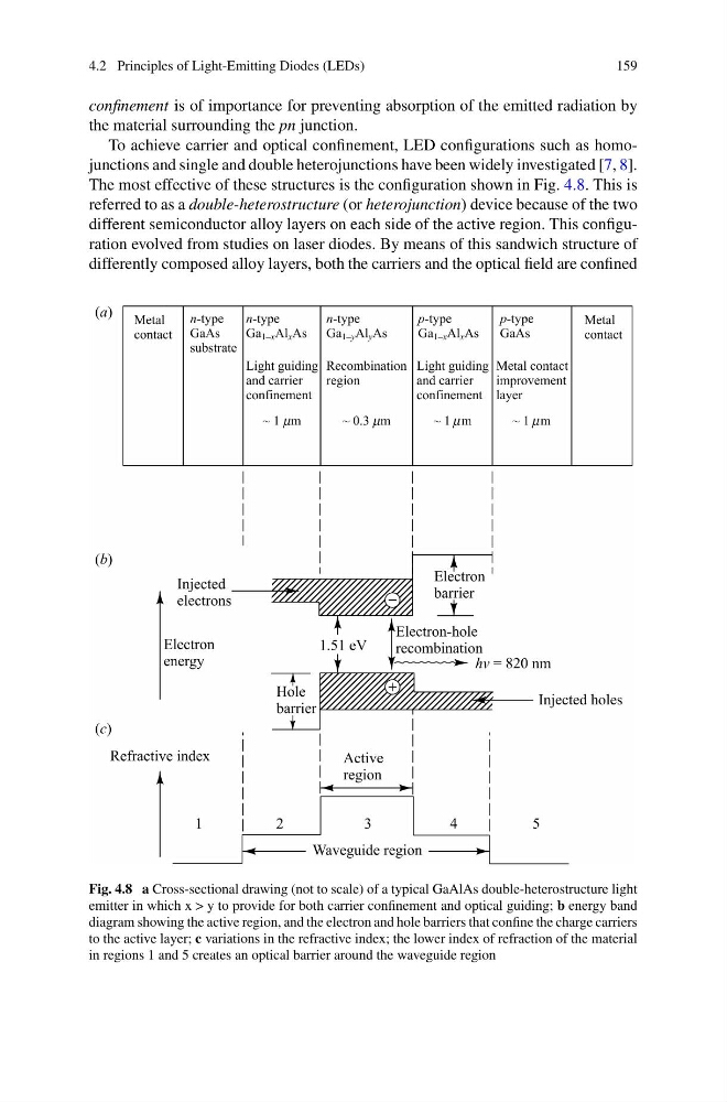
The most effective of these structures is the configuration shown in Fig. 4.8. This is
referred to as a double-heterostructure (or heterojunction) device because of the two
different semiconductor alloy layers on each side of the active region. This configuration evolved from studies on laser diodes. By means of this sandwich structure of
differently composed alloy layers, both the carriers and the optical field are confined
Fig. 4.8 a Cross-sectional drawing (not to scale) of a typical GaAlAs double-heterostructure light
emitter in which x > y to provide for both carrier confinement and optical guiding; b energy band
diagram showing the active region, and the electron and hole barriers that confine the charge carriers
to the active layer; c variations in the refractive index; the lower index of refraction of the material
in regions 1 and 5 creates an optical barrier around the waveguide region
159
confinement is of importance for preventing absorption of the emitted radiation by
the material surrounding the pn junction.
To achieve carrier and optical confinement, LED configurations such as homojunctions and single and double heterojunctions have been widely investigated [7, 8].
The most effective of these structures is the configuration shown in Fig. 4.8. This is
referred to as a double-heterostructure (or heterojunction) device because of the two
different semiconductor alloy layers on each side of the active region. This configuration evolved from studies on laser diodes. By means of this sandwich structure of
differently composed alloy layers, both the carriers and the optical field are confined
Fig. 4.8 a Cross-sectional drawing (not to scale) of a typical GaAlAs double-heterostructure light
emitter in which x > y to provide for both carrier confinement and optical guiding; b energy band
diagram showing the active region, and the electron and hole barriers that confine the charge carriers
to the active layer; c variations in the refractive index; the lower index of refraction of the material
in regions 1 and 5 creates an optical barrier around the waveguide region