

4.1 Basic Concepts of Semiconductor Physics
155
because by definition E = dV /dx. The resulting potential across the pn junction is the
parabolic function shown in Fig. 4.4. The magnitude of the potential varies from 0 to
a maximum value V max , which is called the barrier potential or the built-in potential.
This potential prevents further net movements of charges once equilibrium has been
established. The junction area now has no mobile carriers because its electrons and
holes are locked into a covalent bond structure. This region is called either the
depletion region or the space charge region.
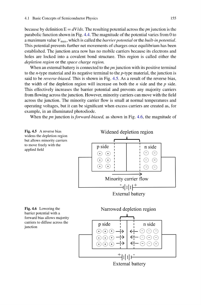
When an external battery is connected to the pn junction with its positive terminal
to the n-type material and its negative terminal to the p-type material, the junction is
said to be reverse-biased. This is shown in Fig. 4.5. As a result of the reverse bias,
the width of the depletion region will increase on both the n side and the p side.
This effectively increases the barrier potential and prevents any majority carriers
from flowing across the junction. However, minority carriers can move with the field
across the junction. The minority carrier flow is small at normal temperatures and
operating voltages, but it can be significant when excess carriers are created as, for
example, in an illuminated photodiode.
When the pn junction is forward-biased, as shown in Fig. 4.6, the magnitude of
Fig. 4.5 A reverse bias
widens the depletion region
but allows minority carriers
to move freely with the
applied field
Fig. 4.6 Lowering the
barrier potential with a
forward bias allows majority
carriers to diffuse across the
junction
155
because by definition E = dV /dx. The resulting potential across the pn junction is the
parabolic function shown in Fig. 4.4. The magnitude of the potential varies from 0 to
a maximum value V max , which is called the barrier potential or the built-in potential.
This potential prevents further net movements of charges once equilibrium has been
established. The junction area now has no mobile carriers because its electrons and
holes are locked into a covalent bond structure. This region is called either the
depletion region or the space charge region.
When an external battery is connected to the pn junction with its positive terminal
to the n-type material and its negative terminal to the p-type material, the junction is
said to be reverse-biased. This is shown in Fig. 4.5. As a result of the reverse bias,
the width of the depletion region will increase on both the n side and the p side.
This effectively increases the barrier potential and prevents any majority carriers
from flowing across the junction. However, minority carriers can move with the field
across the junction. The minority carrier flow is small at normal temperatures and
operating voltages, but it can be significant when excess carriers are created as, for
example, in an illuminated photodiode.
When the pn junction is forward-biased, as shown in Fig. 4.6, the magnitude of
Fig. 4.5 A reverse bias
widens the depletion region
but allows minority carriers
to move freely with the
applied field
Fig. 4.6 Lowering the
barrier potential with a
forward bias allows majority
carriers to diffuse across the
junction