

154
4 Light Sources for Fiber Links
n N =
N D
2
1 +
4n
2
i
N
2
D
+ 1
If n i n D , which is generally the case, then to a good approximation
n N = N D and p N = n
2
i /n D
4.1.3 Concept of a pn Junction
Doped n-type or p-type semiconductor material by itself serves only as a conductor.
To make devices out of these semiconductors, it is necessary to use both types of
materials (in a single, continuous crystal structure). The junction between the two
material regions, which is known as the pn junction, is responsible for the useful
electrical characteristics of a semiconductor device.
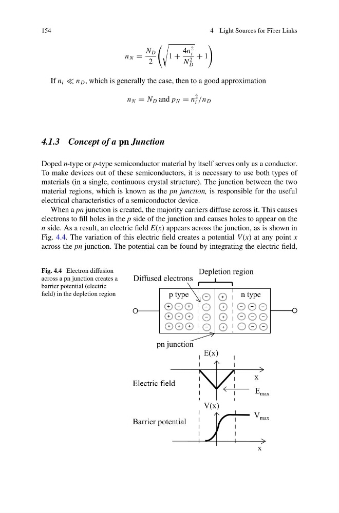
When a pn junction is created, the majority carriers diffuse across it. This causes
electrons to fill holes in the p side of the junction and causes holes to appear on the
n side. As a result, an electric field E(x) appears across the junction, as is shown in
Fig. 4.4. The variation of this electric field creates a potential V (x) at any point x
across the pn junction. The potential can be found by integrating the electric field,
Fig. 4.4 Electron diffusion
across a pn junction creates a
barrier potential (electric
field) in the depletion region
4 Light Sources for Fiber Links
n N =
N D
2
1 +
4n
2
i
N
2
D
+ 1
If n i n D , which is generally the case, then to a good approximation
n N = N D and p N = n
2
i /n D
4.1.3 Concept of a pn Junction
Doped n-type or p-type semiconductor material by itself serves only as a conductor.
To make devices out of these semiconductors, it is necessary to use both types of
materials (in a single, continuous crystal structure). The junction between the two
material regions, which is known as the pn junction, is responsible for the useful
electrical characteristics of a semiconductor device.
When a pn junction is created, the majority carriers diffuse across it. This causes
electrons to fill holes in the p side of the junction and causes holes to appear on the
n side. As a result, an electric field E(x) appears across the junction, as is shown in
Fig. 4.4. The variation of this electric field creates a potential V (x) at any point x
across the pn junction. The potential can be found by integrating the electric field,
Fig. 4.4 Electron diffusion
across a pn junction creates a
barrier potential (electric
field) in the depletion region