

constant applied voltage, the tunneling current, I, is given approximately by
I ≈ e
−2kh
(8.37)
Equation 8.37 tells us that the tunneling current decreases exponentially
as we move the tip away from the surface. The constant k is called
the electronic decay length of the electron and is a measure of how the
probability density of a confined electron decays with distance, or more
precisely, it is the decay length of the electronic wavefunction. Not surprisingly, k depends on how tightly the electron is bound to the conducting surface, called the work function of the surface. The ability of
electrons to travel or “tunnel” through a nonconducting medium between
two conducting materials that are close together is strictly a quantum
mechanical effect, which was previously discussed in Chapter 4 as a
consequence of finite potential energy barriers and involves the wavefunction of electrons penetrating into the classically forbidden region (in
this case, the space between the conductors). As the wavefunction decays
exponentially in the forbidden region, tunneling exhibits an exponential
decay as a function of the distance between the two materials.
As the STM tip is scanned across a rough surface, the tunneling current changes as the tip encounters bumps or dips in the surface (or as h
Z
Y
X
Piezoelectric
transducers
STM tip
Substrate
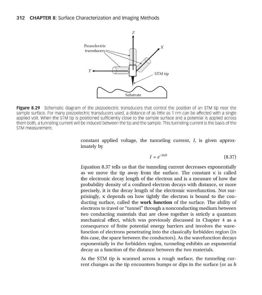
Figure 8.29 Schematic diagram of the piezoelectric transducers that control the position of an STM tip near the
sample surface. For many piezoelectric transducers used, a distance of as little as 1 nm can be affected with a single
applied volt. When the STM tip is positioned sufficiently close to the sample surface and a potential is applied across
them both, a tunneling current will be induced between the tip and the sample. This tunneling current is the basis of the
STM measurement.
CHAPTER 8: Surface Characterization and Imaging Methods
312
I ≈ e
−2kh
(8.37)
Equation 8.37 tells us that the tunneling current decreases exponentially
as we move the tip away from the surface. The constant k is called
the electronic decay length of the electron and is a measure of how the
probability density of a confined electron decays with distance, or more
precisely, it is the decay length of the electronic wavefunction. Not surprisingly, k depends on how tightly the electron is bound to the conducting surface, called the work function of the surface. The ability of
electrons to travel or “tunnel” through a nonconducting medium between
two conducting materials that are close together is strictly a quantum
mechanical effect, which was previously discussed in Chapter 4 as a
consequence of finite potential energy barriers and involves the wavefunction of electrons penetrating into the classically forbidden region (in
this case, the space between the conductors). As the wavefunction decays
exponentially in the forbidden region, tunneling exhibits an exponential
decay as a function of the distance between the two materials.
As the STM tip is scanned across a rough surface, the tunneling current changes as the tip encounters bumps or dips in the surface (or as h
Z
Y
X
Piezoelectric
transducers
STM tip
Substrate
Figure 8.29 Schematic diagram of the piezoelectric transducers that control the position of an STM tip near the
sample surface. For many piezoelectric transducers used, a distance of as little as 1 nm can be affected with a single
applied volt. When the STM tip is positioned sufficiently close to the sample surface and a potential is applied across
them both, a tunneling current will be induced between the tip and the sample. This tunneling current is the basis of the
STM measurement.
CHAPTER 8: Surface Characterization and Imaging Methods
312