

302 12 Characterization of Nanomaterials
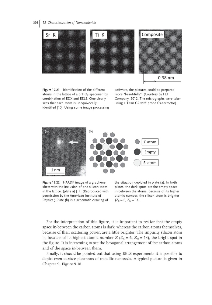
For the interpretation of this figure, it is important to realize that the empty
space in-between the carbon atoms is dark, whereas the carbon atoms themselves,
because of their scattering power, are a little brighter. The impurity silicon atom
is, because of its highest atomic number Z (Z C = 6, Z Si = 14), the bright spot in
the figure. It is interesting to see the hexagonal arrangement of the carbon atoms
and of the space in-between them.
Finally, it should be pointed out that using EELS experiments it is possible to
depict even surface plasmons of metallic nanorods. A typical picture is given in
Chapter 9, Figure 9.18.
Figure 12.21 Identification of the different
atoms in the lattice of a SrTiO 3 specimen by
combination of EDX and EELS. One clearly
sees that each atom is unequivocally
identified [10]. Using some image processing
software, the pictures could be prepared
more “beautifully”. (Courtesy by FEI
Company, 2012. The micrographs were taken
using a Titan G2 with probe Cs-corrector).
Ti K
Sr K
Composite
0.38 nm
Figure 12.22 HAADF image of a graphene
sheet with the inclusion of one silicon atom
in the lattice. (plate a) [11] (Reproduced with
permission by the American Institute of
Physics.) Plate (b) is a schematic drawing of
the situation depicted in plate (a). In both
plates: the dark spots are the empty space
in-between the atoms, because of its higher
atomic number, the silicon atom is brighter
(Z C = 6, Z Si = 14).
C atom
Empty
Si atom
1 nm
(a)
(b)
For the interpretation of this figure, it is important to realize that the empty
space in-between the carbon atoms is dark, whereas the carbon atoms themselves,
because of their scattering power, are a little brighter. The impurity silicon atom
is, because of its highest atomic number Z (Z C = 6, Z Si = 14), the bright spot in
the figure. It is interesting to see the hexagonal arrangement of the carbon atoms
and of the space in-between them.
Finally, it should be pointed out that using EELS experiments it is possible to
depict even surface plasmons of metallic nanorods. A typical picture is given in
Chapter 9, Figure 9.18.
Figure 12.21 Identification of the different
atoms in the lattice of a SrTiO 3 specimen by
combination of EDX and EELS. One clearly
sees that each atom is unequivocally
identified [10]. Using some image processing
software, the pictures could be prepared
more “beautifully”. (Courtesy by FEI
Company, 2012. The micrographs were taken
using a Titan G2 with probe Cs-corrector).
Ti K
Sr K
Composite
0.38 nm
Figure 12.22 HAADF image of a graphene
sheet with the inclusion of one silicon atom
in the lattice. (plate a) [11] (Reproduced with
permission by the American Institute of
Physics.) Plate (b) is a schematic drawing of
the situation depicted in plate (a). In both
plates: the dark spots are the empty space
in-between the atoms, because of its higher
atomic number, the silicon atom is brighter
(Z C = 6, Z Si = 14).
C atom
Empty
Si atom
1 nm
(a)
(b)