

298 12 Characterization of Nanomaterials
difficult.) This is useful, provided the crystallographic orientation is characterized
by low Miller indices, to determine the crystallographic structure of the specimen.
By tilting the specimen, changing the orientation of the specimen with respect to
the electron beam, it is possible to obtain additional structural information.
Electron microscopes using a system to correct spherical aberration do not need
extremely high voltages to obtain atomic resolution. Figure 12.17 displays an
example. This micrograph, taken at 80 kV acceleration voltage displays a sheet of
graphene. One sees the hexagons, which are structuring elements of graphene.
This is exactly the image that is expected from the theoretical considerations and
depicted as sketched in Figure 5.11. One of these hexagons, placed in a white
circle, is highlighted by dark points. The distance between two of these points is
0.14 nm.
When analyzing a specimen in an electron microscope, sometimes it is advised
to change between the bright-field and the dark-field mode. By varying tilting angle
and rotation, one sees quite rapidly if a material contains crystalline grains or not.
In dark field electron microscopy, those crystallized particles that are in the proper
orientation to the electron beam appear bright. A typical example is displayed in
Figure 12.18.
The specimen used for Figure 12.18 consisted of amorphous alumina with
small zirconia precipitates. The bright spots visible in the dark-field micrograph,
plate (b), indicate that the specimen contains crystallized particles. Changing the
tilting angle and the rotation of the incident electron beam produces other bright
spots, depending in the crystallographic orientation with respect to the electron
beam.
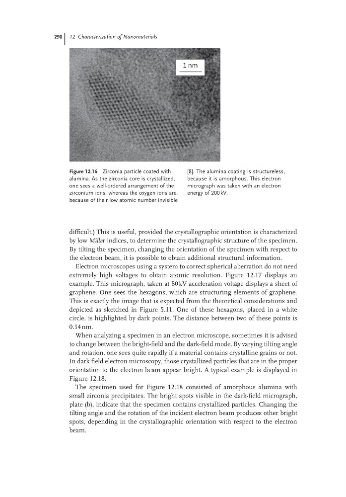
Figure 12.16 Zirconia particle coated with
alumina. As the zirconia core is crystallized,
one sees a well-ordered arrangement of the
zirconium ions; whereas the oxygen ions are,
because of their low atomic number invisible
[8]. The alumina coating is structureless,
because it is amorphous. This electron
micrograph was taken with an electron
energy of 200 kV.
1 nm
difficult.) This is useful, provided the crystallographic orientation is characterized
by low Miller indices, to determine the crystallographic structure of the specimen.
By tilting the specimen, changing the orientation of the specimen with respect to
the electron beam, it is possible to obtain additional structural information.
Electron microscopes using a system to correct spherical aberration do not need
extremely high voltages to obtain atomic resolution. Figure 12.17 displays an
example. This micrograph, taken at 80 kV acceleration voltage displays a sheet of
graphene. One sees the hexagons, which are structuring elements of graphene.
This is exactly the image that is expected from the theoretical considerations and
depicted as sketched in Figure 5.11. One of these hexagons, placed in a white
circle, is highlighted by dark points. The distance between two of these points is
0.14 nm.
When analyzing a specimen in an electron microscope, sometimes it is advised
to change between the bright-field and the dark-field mode. By varying tilting angle
and rotation, one sees quite rapidly if a material contains crystalline grains or not.
In dark field electron microscopy, those crystallized particles that are in the proper
orientation to the electron beam appear bright. A typical example is displayed in
Figure 12.18.
The specimen used for Figure 12.18 consisted of amorphous alumina with
small zirconia precipitates. The bright spots visible in the dark-field micrograph,
plate (b), indicate that the specimen contains crystallized particles. Changing the
tilting angle and the rotation of the incident electron beam produces other bright
spots, depending in the crystallographic orientation with respect to the electron
beam.
Figure 12.16 Zirconia particle coated with
alumina. As the zirconia core is crystallized,
one sees a well-ordered arrangement of the
zirconium ions; whereas the oxygen ions are,
because of their low atomic number invisible
[8]. The alumina coating is structureless,
because it is amorphous. This electron
micrograph was taken with an electron
energy of 200 kV.
1 nm