

10.3 Other One-Dimensional Electrical Conductors 239
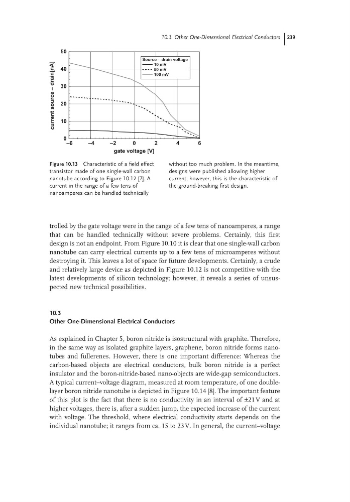
trolled by the gate voltage were in the range of a few tens of nanoamperes, a range
that can be handled technically without severe problems. Certainly, this first
design is not an endpoint. From Figure 10.10 it is clear that one single-wall carbon
nanotube can carry electrical currents up to a few tens of microamperes without
destroying it. This leaves a lot of space for future developments. Certainly, a crude
and relatively large device as depicted in Figure 10.12 is not competitive with the
latest developments of silicon technology; however, it reveals a series of unsuspected new technical possibilities.
10.3
Other One-Dimensional Electrical Conductors
As explained in Chapter 5, boron nitride is isostructural with graphite. Therefore,
in the same way as isolated graphite layers, graphene, boron nitride forms nanotubes and fullerenes. However, there is one important difference: Whereas the
carbon-based objects are electrical conductors, bulk boron nitride is a perfect
insulator and the boron-nitride-based nano-objects are wide-gap semiconductors.
A typical current–voltage diagram, measured at room temperature, of one doublelayer boron nitride nanotube is depicted in Figure 10.14 [8]. The important feature
of this plot is the fact that there is no conductivity in an interval of ±21 V and at
higher voltages, there is, after a sudden jump, the expected increase of the current
with voltage. The threshold, where electrical conductivity starts depends on the
individual nanotube; it ranges from ca. 15 to 23 V. In general, the current–voltage
Figure 10.13 Characteristic of a field effect
transistor made of one single-wall carbon
nanotube according to Figure 10.12 [7]. A
current in the range of a few tens of
nanoamperes can be handled technically
without too much problem. In the meantime,
designs were published allowing higher
current; however, this is the characteristic of
the ground-breaking first design.
–6
–4
–2
0
2
4
6
gate voltage [V]
0
10
20
30
40
50
current
source
–
drain[nA]
Source – drain voltage
10 mV
50 mV
100 mV
trolled by the gate voltage were in the range of a few tens of nanoamperes, a range
that can be handled technically without severe problems. Certainly, this first
design is not an endpoint. From Figure 10.10 it is clear that one single-wall carbon
nanotube can carry electrical currents up to a few tens of microamperes without
destroying it. This leaves a lot of space for future developments. Certainly, a crude
and relatively large device as depicted in Figure 10.12 is not competitive with the
latest developments of silicon technology; however, it reveals a series of unsuspected new technical possibilities.
10.3
Other One-Dimensional Electrical Conductors
As explained in Chapter 5, boron nitride is isostructural with graphite. Therefore,
in the same way as isolated graphite layers, graphene, boron nitride forms nanotubes and fullerenes. However, there is one important difference: Whereas the
carbon-based objects are electrical conductors, bulk boron nitride is a perfect
insulator and the boron-nitride-based nano-objects are wide-gap semiconductors.
A typical current–voltage diagram, measured at room temperature, of one doublelayer boron nitride nanotube is depicted in Figure 10.14 [8]. The important feature
of this plot is the fact that there is no conductivity in an interval of ±21 V and at
higher voltages, there is, after a sudden jump, the expected increase of the current
with voltage. The threshold, where electrical conductivity starts depends on the
individual nanotube; it ranges from ca. 15 to 23 V. In general, the current–voltage
Figure 10.13 Characteristic of a field effect
transistor made of one single-wall carbon
nanotube according to Figure 10.12 [7]. A
current in the range of a few tens of
nanoamperes can be handled technically
without too much problem. In the meantime,
designs were published allowing higher
current; however, this is the characteristic of
the ground-breaking first design.
–6
–4
–2
0
2
4
6
gate voltage [V]
0
10
20
30
40
50
current
source
–
drain[nA]
Source – drain voltage
10 mV
50 mV
100 mV