

238 10 Electrical Properties
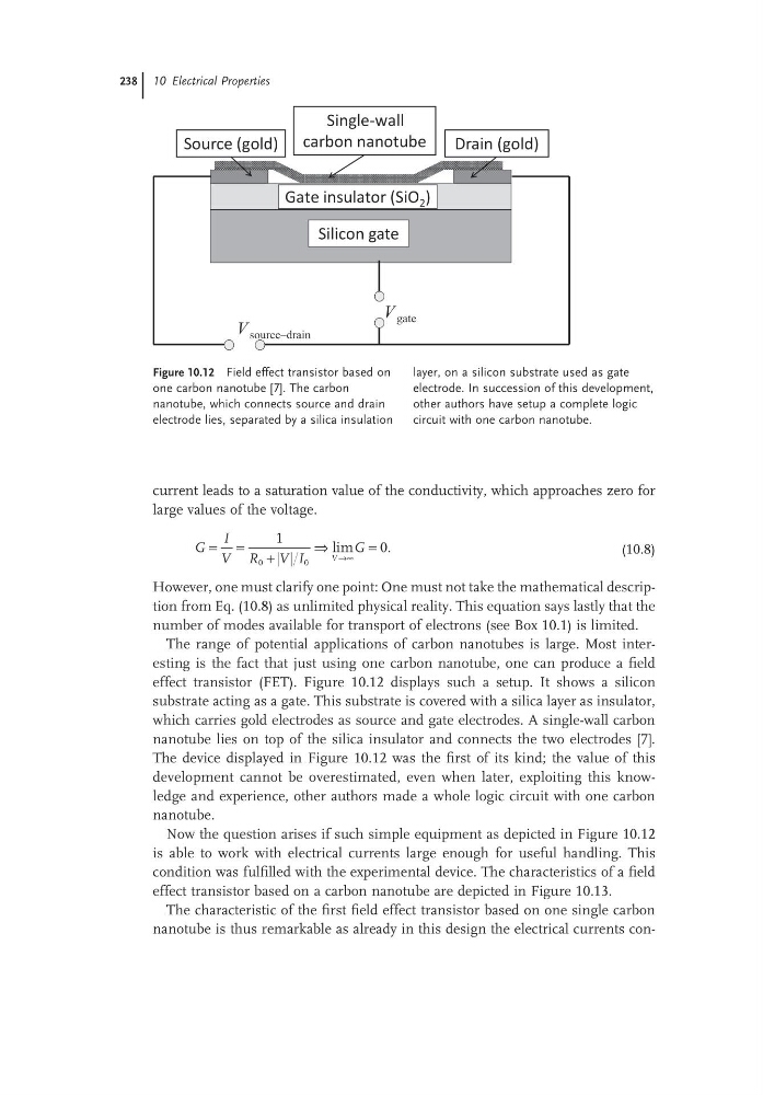
Figure 10.12 Field effect transistor based on
one carbon nanotube [7]. The carbon
nanotube, which connects source and drain
electrode lies, separated by a silica insulation
layer, on a silicon substrate used as gate
electrode. In succession of this development,
other authors have setup a complete logic
circuit with one carbon nanotube.
V source–drain
Silicon gate
Gate insulator (SiO 2 )
Single-wall
carbon nanotube
Source (gold)
Drain (gold)
V gate
current leads to a saturation value of the conductivity, which approaches zero for
large values of the voltage.
G
I
V R V I
G
V
= =
+
⇒
=
→∞
1
0
0
0
lim
.
(10.8)
However, one must clarify one point: One must not take the mathematical description from Eq. (10.8) as unlimited physical reality. This equation says lastly that the
number of modes available for transport of electrons (see Box 10.1) is limited.
The range of potential applications of carbon nanotubes is large. Most interesting is the fact that just using one carbon nanotube, one can produce a field
effect transistor (FET). Figure 10.12 displays such a setup. It shows a silicon
substrate acting as a gate. This substrate is covered with a silica layer as insulator,
which carries gold electrodes as source and gate electrodes. A single-wall carbon
nanotube lies on top of the silica insulator and connects the two electrodes [7].
The device displayed in Figure 10.12 was the first of its kind; the value of this
development cannot be overestimated, even when later, exploiting this knowledge and experience, other authors made a whole logic circuit with one carbon
nanotube.
Now the question arises if such simple equipment as depicted in Figure 10.12
is able to work with electrical currents large enough for useful handling. This
condition was fulfilled with the experimental device. The characteristics of a field
effect transistor based on a carbon nanotube are depicted in Figure 10.13.
The characteristic of the first field effect transistor based on one single carbon
nanotube is thus remarkable as already in this design the electrical currents con-
Figure 10.12 Field effect transistor based on
one carbon nanotube [7]. The carbon
nanotube, which connects source and drain
electrode lies, separated by a silica insulation
layer, on a silicon substrate used as gate
electrode. In succession of this development,
other authors have setup a complete logic
circuit with one carbon nanotube.
V source–drain
Silicon gate
Gate insulator (SiO 2 )
Single-wall
carbon nanotube
Source (gold)
Drain (gold)
V gate
current leads to a saturation value of the conductivity, which approaches zero for
large values of the voltage.
G
I
V R V I
G
V
= =
+
⇒
=
→∞
1
0
0
0
lim
.
(10.8)
However, one must clarify one point: One must not take the mathematical description from Eq. (10.8) as unlimited physical reality. This equation says lastly that the
number of modes available for transport of electrons (see Box 10.1) is limited.
The range of potential applications of carbon nanotubes is large. Most interesting is the fact that just using one carbon nanotube, one can produce a field
effect transistor (FET). Figure 10.12 displays such a setup. It shows a silicon
substrate acting as a gate. This substrate is covered with a silica layer as insulator,
which carries gold electrodes as source and gate electrodes. A single-wall carbon
nanotube lies on top of the silica insulator and connects the two electrodes [7].
The device displayed in Figure 10.12 was the first of its kind; the value of this
development cannot be overestimated, even when later, exploiting this knowledge and experience, other authors made a whole logic circuit with one carbon
nanotube.
Now the question arises if such simple equipment as depicted in Figure 10.12
is able to work with electrical currents large enough for useful handling. This
condition was fulfilled with the experimental device. The characteristics of a field
effect transistor based on a carbon nanotube are depicted in Figure 10.13.
The characteristic of the first field effect transistor based on one single carbon
nanotube is thus remarkable as already in this design the electrical currents con-