

314
V. Melnik et al.
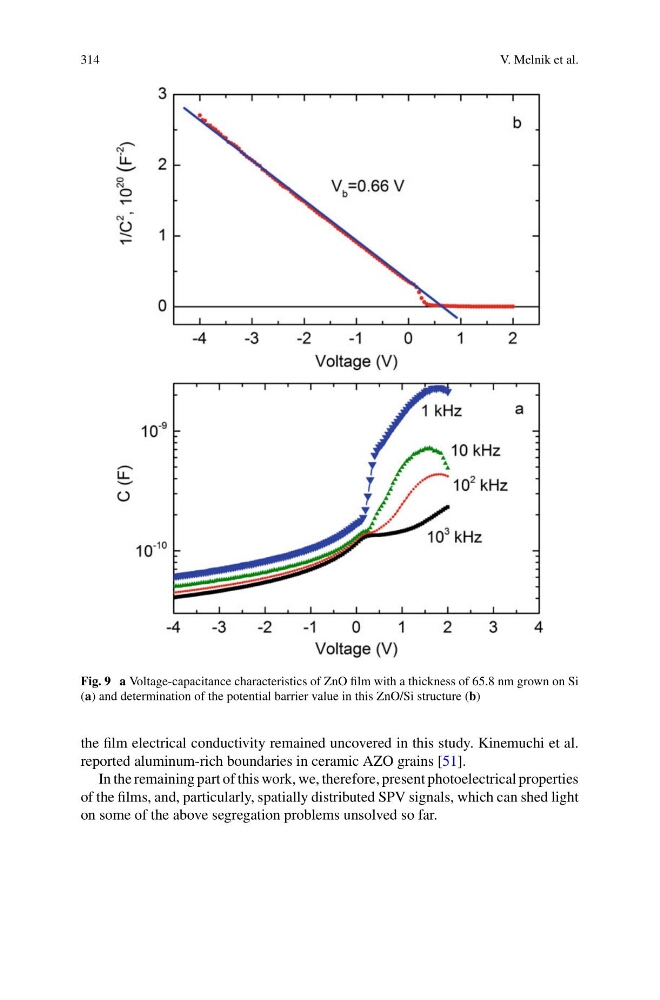
Fig. 9 a Voltage-capacitance characteristics of ZnO film with a thickness of 65.8 nm grown on Si
(a) and determination of the potential barrier value in this ZnO/Si structure (b)
the film electrical conductivity remained uncovered in this study. Kinemuchi et al.
reported aluminum-rich boundaries in ceramic AZO grains [51].
In the remaining part of this work, we, therefore, present photoelectrical properties
of the films, and, particularly, spatially distributed SPV signals, which can shed light
on some of the above segregation problems unsolved so far.
V. Melnik et al.
Fig. 9 a Voltage-capacitance characteristics of ZnO film with a thickness of 65.8 nm grown on Si
(a) and determination of the potential barrier value in this ZnO/Si structure (b)
the film electrical conductivity remained uncovered in this study. Kinemuchi et al.
reported aluminum-rich boundaries in ceramic AZO grains [51].
In the remaining part of this work, we, therefore, present photoelectrical properties
of the films, and, particularly, spatially distributed SPV signals, which can shed light
on some of the above segregation problems unsolved so far.