

Formation and Transient Photovoltaic Properties of ZnO/Si …
313
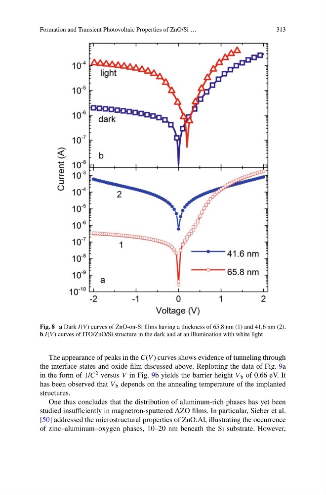
Fig. 8 a Dark I(V ) curves of ZnO-on-Si films having a thickness of 65.8 nm (1) and 41.6 nm (2).
b I(V ) curves of ITO/ZnO/Si structure in the dark and at an illumination with white light
The appearance of peaks in the C(V ) curves shows evidence of tunneling through
the interface states and oxide film discussed above. Replotting the data of Fig. 9a
in the form of 1/C
2 versus V in Fig. 9b yields the barrier height V b of 0.66 eV. It
has been observed that V b depends on the annealing temperature of the implanted
structures.
One thus concludes that the distribution of aluminum-rich phases has yet been
studied insufficiently in magnetron-sputtered AZO films. In particular, Sieber et al.
[50] addressed the microstructural properties of ZnO:Al, illustrating the occurrence
of zinc–aluminum–oxygen phases, 10–20 nm beneath the Si substrate. However,
313
Fig. 8 a Dark I(V ) curves of ZnO-on-Si films having a thickness of 65.8 nm (1) and 41.6 nm (2).
b I(V ) curves of ITO/ZnO/Si structure in the dark and at an illumination with white light
The appearance of peaks in the C(V ) curves shows evidence of tunneling through
the interface states and oxide film discussed above. Replotting the data of Fig. 9a
in the form of 1/C
2 versus V in Fig. 9b yields the barrier height V b of 0.66 eV. It
has been observed that V b depends on the annealing temperature of the implanted
structures.
One thus concludes that the distribution of aluminum-rich phases has yet been
studied insufficiently in magnetron-sputtered AZO films. In particular, Sieber et al.
[50] addressed the microstructural properties of ZnO:Al, illustrating the occurrence
of zinc–aluminum–oxygen phases, 10–20 nm beneath the Si substrate. However,