

Formation and Transient Photovoltaic Properties of ZnO/Si …
309
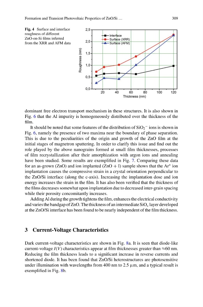
Fig. 4 Surface and interface
roughness of different
ZnO-on-Si films inferred
from the XRR and AFM data
dominant free electron transport mechanism in these structures. It is also shown in
Fig. 6 that the Al impurity is homogeneously distributed over the thickness of the
film.
It should be noted that some features of the distribution of SiO 2
− ions is shown in
Fig. 6, namely the presence of two maxima near the boundary of phase separation.
This is due to the peculiarities of the origin and growth of the ZnO film at the
initial stages of magnetron sputtering. In order to clarify this issue and find out the
role played by the above nanograins formed at small film thicknesses, processes
of film recrystallization after their amorphization with argon ions and annealing
have been studied. Some results are exemplified in Fig. 7. Comparing these data
for an as-grown (ZnO) and ion implanted (ZnO + I) sample shows that the Ar
+ ion
implantation causes the compressive strain in a crystal orientation perpendicular to
the ZnO/Si interface (along the c-axis). Increasing the implantation dose and ion
energy increases the strain in the film. It has also been verified that the thickness of
the films decreases somewhat upon implantation due to decreased inter-grain spacing
while their porosity concomitantly increases.
Adding Al during the growth tightens the film, enhances the electrical conductivity
and varies the bandgap of ZnO. The thickness of an intermediate SiO x layer developed
at the ZnO/Si interface has been found to be nearly independent of the film thickness.
3 Current-Voltage Characteristics
Dark current-voltage characteristics are shown in Fig. 8a. It is seen that diode-like
current-voltage I(V ) characteristics appear at film thicknesses greater than ≈60 nm.
Reducing the film thickness leads to a significant increase in reverse currents and
shortened diode. It has been found that ZnO/Si heterostructures are photosensitive
under illumination with wavelengths from 400 nm to 2.5 μm, and a typical result is
exemplified in Fig. 8b.
309
Fig. 4 Surface and interface
roughness of different
ZnO-on-Si films inferred
from the XRR and AFM data
dominant free electron transport mechanism in these structures. It is also shown in
Fig. 6 that the Al impurity is homogeneously distributed over the thickness of the
film.
It should be noted that some features of the distribution of SiO 2
− ions is shown in
Fig. 6, namely the presence of two maxima near the boundary of phase separation.
This is due to the peculiarities of the origin and growth of the ZnO film at the
initial stages of magnetron sputtering. In order to clarify this issue and find out the
role played by the above nanograins formed at small film thicknesses, processes
of film recrystallization after their amorphization with argon ions and annealing
have been studied. Some results are exemplified in Fig. 7. Comparing these data
for an as-grown (ZnO) and ion implanted (ZnO + I) sample shows that the Ar
+ ion
implantation causes the compressive strain in a crystal orientation perpendicular to
the ZnO/Si interface (along the c-axis). Increasing the implantation dose and ion
energy increases the strain in the film. It has also been verified that the thickness of
the films decreases somewhat upon implantation due to decreased inter-grain spacing
while their porosity concomitantly increases.
Adding Al during the growth tightens the film, enhances the electrical conductivity
and varies the bandgap of ZnO. The thickness of an intermediate SiO x layer developed
at the ZnO/Si interface has been found to be nearly independent of the film thickness.
3 Current-Voltage Characteristics
Dark current-voltage characteristics are shown in Fig. 8a. It is seen that diode-like
current-voltage I(V ) characteristics appear at film thicknesses greater than ≈60 nm.
Reducing the film thickness leads to a significant increase in reverse currents and
shortened diode. It has been found that ZnO/Si heterostructures are photosensitive
under illumination with wavelengths from 400 nm to 2.5 μm, and a typical result is
exemplified in Fig. 8b.