

Formation and Transient Photovoltaic Properties of ZnO/Si …
307
Upon increasing the thickness to about 67 nm, the three ZnO fingerprints could be
clearly resolved on a semi-log scale of the XRD spectrum. This may be due to the
weakening of the influence of the substrate, which thus changes the internal structure
of the films. At the film thicknesses of 120 nm, the (101) and (100) peaks gain in
intensity.
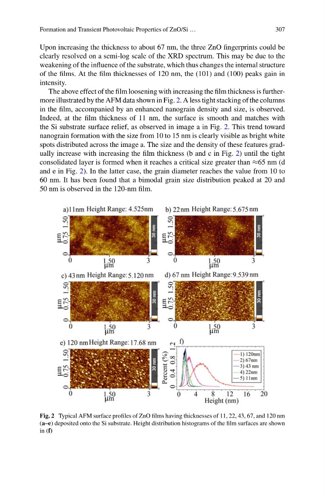
The above effect of the film loosening with increasing the film thickness is furthermore illustrated by the AFM data shown in Fig. 2. A less tight stacking of the columns
in the film, accompanied by an enhanced nanograin density and size, is observed.
Indeed, at the film thickness of 11 nm, the surface is smooth and matches with
the Si substrate surface relief, as observed in image a in Fig. 2. This trend toward
nanograin formation with the size from 10 to 15 nm is clearly visible as bright white
spots distributed across the image a. The size and the density of these features gradually increase with increasing the film thickness (b and c in Fig. 2) until the tight
consolidated layer is formed when it reaches a critical size greater than ≈65 nm (d
and e in Fig. 2). In the latter case, the grain diameter reaches the value from 10 to
60 nm. It has been found that a bimodal grain size distribution peaked at 20 and
50 nm is observed in the 120-nm film.
Fig. 2 Typical AFM surface profiles of ZnO films having thicknesses of 11, 22, 43, 67, and 120 nm
(a–e) deposited onto the Si substrate. Height distribution histograms of the film surfaces are shown
in (f)
307
Upon increasing the thickness to about 67 nm, the three ZnO fingerprints could be
clearly resolved on a semi-log scale of the XRD spectrum. This may be due to the
weakening of the influence of the substrate, which thus changes the internal structure
of the films. At the film thicknesses of 120 nm, the (101) and (100) peaks gain in
intensity.
The above effect of the film loosening with increasing the film thickness is furthermore illustrated by the AFM data shown in Fig. 2. A less tight stacking of the columns
in the film, accompanied by an enhanced nanograin density and size, is observed.
Indeed, at the film thickness of 11 nm, the surface is smooth and matches with
the Si substrate surface relief, as observed in image a in Fig. 2. This trend toward
nanograin formation with the size from 10 to 15 nm is clearly visible as bright white
spots distributed across the image a. The size and the density of these features gradually increase with increasing the film thickness (b and c in Fig. 2) until the tight
consolidated layer is formed when it reaches a critical size greater than ≈65 nm (d
and e in Fig. 2). In the latter case, the grain diameter reaches the value from 10 to
60 nm. It has been found that a bimodal grain size distribution peaked at 20 and
50 nm is observed in the 120-nm film.
Fig. 2 Typical AFM surface profiles of ZnO films having thicknesses of 11, 22, 43, 67, and 120 nm
(a–e) deposited onto the Si substrate. Height distribution histograms of the film surfaces are shown
in (f)