

84
V. L. Borblik
ΔE c
E c2
E c1
E F2
E g1
1
2
E g2
E F1
E v1
ΔE v
E v2
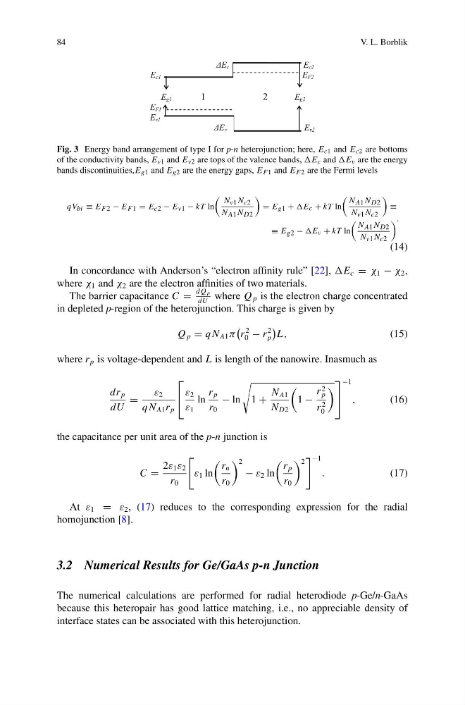
Fig. 3 Energy band arrangement of type I for p-n heterojunction; here, E c1 and E c2 are bottoms
of the conductivity bands, E v1 and E v2 are tops of the valence bands, c and v are the energy
bands discontinuities,E g1 and E g2 are the energy gaps, E F1 and E F2 are the Fermi levels
qV bi ≡ E F2 − E F1 = E c2 − E v1 − kT ln
N v1 N c2
N A1 N D2
= E g1 + c + kT ln
N A1 N D2
N v1 N c2
≡
≡ E g2 − v + kT ln
N A1 N D2
N v1 N c2
.
(14)
In concordance with Anderson’s “electron affinity rule” [22], c = χ 1 − χ 2 ,
where χ 1 and χ 2 are the electron affinities of two materials.
The barrier capacitance C =
d Q p
dU
where Q p is the electron charge concentrated
in depleted p-region of the heterojunction. This charge is given by
Q p = q N A1 π
r
2
0 − r
2
p
L ,
(15)
where r p is voltage-dependent and L is length of the nanowire. Inasmuch as
dr p
dU
=
ε 2
q N A1 r p
⎡
⎣ ε 2
ε 1
ln
r p
r 0
− ln
1 +
N A1
N D2
1 −
r 2
p
r
2
0
⎤
⎦
−1
,
(16)
the capacitance per unit area of the p-n junction is
C =
2ε 1 ε 2
r 0
ε 1 ln
r n
r 0
2
− ε 2 ln
r p
r 0
2
−1
.
(17)
At ε 1 = ε 2 , (17) reduces to the corresponding expression for the radial
homojunction [8].
3.2 Numerical Results for Ge/GaAs p-n Junction
The numerical calculations are performed for radial heterodiode p-Ge/n-GaAs
because this heteropair has good lattice matching, i.e., no appreciable density of
interface states can be associated with this heterojunction.
V. L. Borblik
ΔE c
E c2
E c1
E F2
E g1
1
2
E g2
E F1
E v1
ΔE v
E v2
Fig. 3 Energy band arrangement of type I for p-n heterojunction; here, E c1 and E c2 are bottoms
of the conductivity bands, E v1 and E v2 are tops of the valence bands, c and v are the energy
bands discontinuities,E g1 and E g2 are the energy gaps, E F1 and E F2 are the Fermi levels
qV bi ≡ E F2 − E F1 = E c2 − E v1 − kT ln
N v1 N c2
N A1 N D2
= E g1 + c + kT ln
N A1 N D2
N v1 N c2
≡
≡ E g2 − v + kT ln
N A1 N D2
N v1 N c2
.
(14)
In concordance with Anderson’s “electron affinity rule” [22], c = χ 1 − χ 2 ,
where χ 1 and χ 2 are the electron affinities of two materials.
The barrier capacitance C =
d Q p
dU
where Q p is the electron charge concentrated
in depleted p-region of the heterojunction. This charge is given by
Q p = q N A1 π
r
2
0 − r
2
p
L ,
(15)
where r p is voltage-dependent and L is length of the nanowire. Inasmuch as
dr p
dU
=
ε 2
q N A1 r p
⎡
⎣ ε 2
ε 1
ln
r p
r 0
− ln
1 +
N A1
N D2
1 −
r 2
p
r
2
0
⎤
⎦
−1
,
(16)
the capacitance per unit area of the p-n junction is
C =
2ε 1 ε 2
r 0
ε 1 ln
r n
r 0
2
− ε 2 ln
r p
r 0
2
−1
.
(17)
At ε 1 = ε 2 , (17) reduces to the corresponding expression for the radial
homojunction [8].
3.2 Numerical Results for Ge/GaAs p-n Junction
The numerical calculations are performed for radial heterodiode p-Ge/n-GaAs
because this heteropair has good lattice matching, i.e., no appreciable density of
interface states can be associated with this heterojunction.