

106
I. Ivanenko et al.
S
S
Mo
a
b
Mo
S
a
S
S
S
S
S
S
Mo
Mo
Mo
c
a=3.15Å c=12.30Å
1.54Å
1.54Å
1.54Å
1.54Å
1.54Å
1.54Å
3.08Å
3.08Å
S
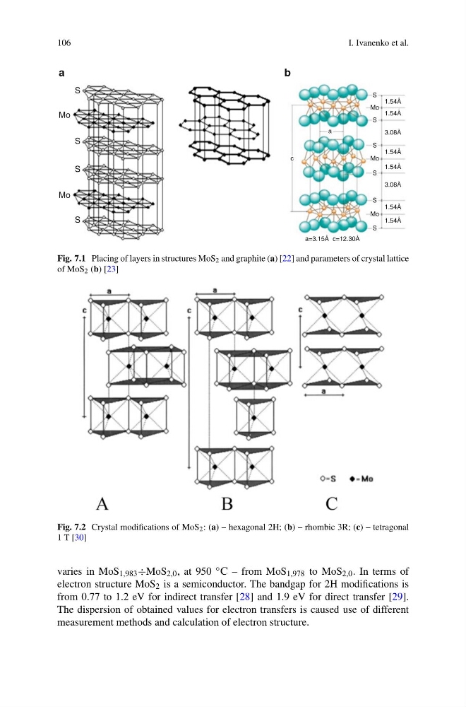
Fig. 7.1 Placing of layers in structures MoS 2 and graphite (a) [22] and parameters of crystal lattice
of MoS 2 (b) [23]
Fig. 7.2 Crystal modifications of MoS 2 : (a) – hexagonal 2H; (b) – rhombic 3R; (c) – tetragonal
1 T [30]
varies in MoS 1,983 ÷MoS 2,0 , at 950 ◦ ´ – from MoS 1,978 to MoS 2,0 . In terms of
electron structure MoS 2 is a semiconductor. The bandgap for 2H modifications is
from 0.77 to 1.2 eV for indirect transfer [28] and 1.9 eV for direct transfer [29].
The dispersion of obtained values for electron transfers is caused use of different
measurement methods and calculation of electron structure.
I. Ivanenko et al.
S
S
Mo
a
b
Mo
S
a
S
S
S
S
S
S
Mo
Mo
Mo
c
a=3.15Å c=12.30Å
1.54Å
1.54Å
1.54Å
1.54Å
1.54Å
1.54Å
3.08Å
3.08Å
S
Fig. 7.1 Placing of layers in structures MoS 2 and graphite (a) [22] and parameters of crystal lattice
of MoS 2 (b) [23]
Fig. 7.2 Crystal modifications of MoS 2 : (a) – hexagonal 2H; (b) – rhombic 3R; (c) – tetragonal
1 T [30]
varies in MoS 1,983 ÷MoS 2,0 , at 950 ◦ ´ – from MoS 1,978 to MoS 2,0 . In terms of
electron structure MoS 2 is a semiconductor. The bandgap for 2H modifications is
from 0.77 to 1.2 eV for indirect transfer [28] and 1.9 eV for direct transfer [29].
The dispersion of obtained values for electron transfers is caused use of different
measurement methods and calculation of electron structure.