

Terahertz Radiation from Gallium Phosphide …
53
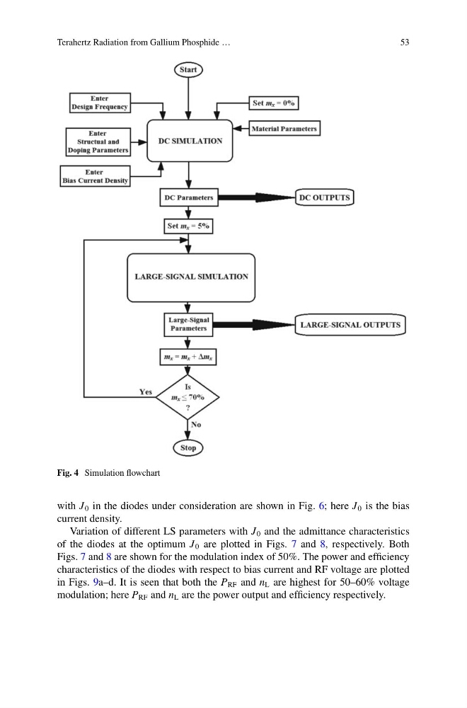
Fig. 4 Simulation flowchart
with J 0 in the diodes under consideration are shown in Fig. 6; here J 0 is the bias
current density.
Variation of different LS parameters with J 0 and the admittance characteristics
of the diodes at the optimum J 0 are plotted in Figs. 7 and 8, respectively. Both
Figs. 7 and 8 are shown for the modulation index of 50%. The power and efficiency
characteristics of the diodes with respect to bias current and RF voltage are plotted
in Figs. 9a–d. It is seen that both the P RF and n L are highest for 50–60% voltage
modulation; here P RF and n L are the power output and efficiency respectively.
53
Fig. 4 Simulation flowchart
with J 0 in the diodes under consideration are shown in Fig. 6; here J 0 is the bias
current density.
Variation of different LS parameters with J 0 and the admittance characteristics
of the diodes at the optimum J 0 are plotted in Figs. 7 and 8, respectively. Both
Figs. 7 and 8 are shown for the modulation index of 50%. The power and efficiency
characteristics of the diodes with respect to bias current and RF voltage are plotted
in Figs. 9a–d. It is seen that both the P RF and n L are highest for 50–60% voltage
modulation; here P RF and n L are the power output and efficiency respectively.