

44
A. Deyasi and A. Sarkar
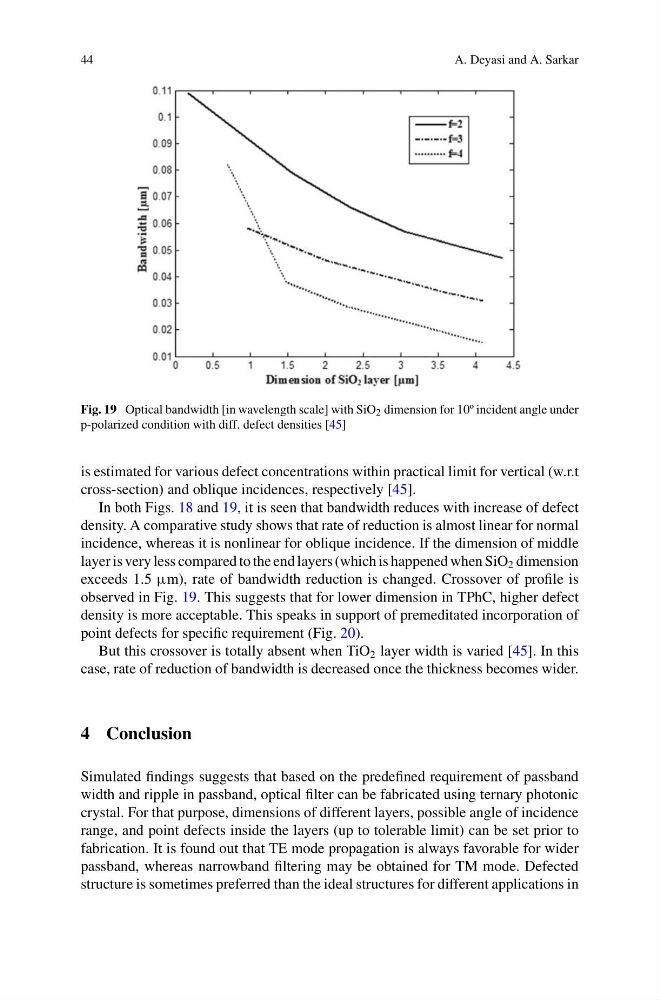
Fig. 19 Optical bandwidth [in wavelength scale] with SiO 2 dimension for 10º incident angle under
p-polarized condition with diff. defect densities [45]
is estimated for various defect concentrations within practical limit for vertical (w.r.t
cross-section) and oblique incidences, respectively [45].
In both Figs. 18 and 19, it is seen that bandwidth reduces with increase of defect
density. A comparative study shows that rate of reduction is almost linear for normal
incidence, whereas it is nonlinear for oblique incidence. If the dimension of middle
layer is very less compared to the end layers (which is happened when SiO 2 dimension
exceeds 1.5 µm), rate of bandwidth reduction is changed. Crossover of profile is
observed in Fig. 19. This suggests that for lower dimension in TPhC, higher defect
density is more acceptable. This speaks in support of premeditated incorporation of
point defects for specific requirement (Fig. 20).
But this crossover is totally absent when TiO 2 layer width is varied [45]. In this
case, rate of reduction of bandwidth is decreased once the thickness becomes wider.
4 Conclusion
Simulated findings suggests that based on the predefined requirement of passband
width and ripple in passband, optical filter can be fabricated using ternary photonic
crystal. For that purpose, dimensions of different layers, possible angle of incidence
range, and point defects inside the layers (up to tolerable limit) can be set prior to
fabrication. It is found out that TE mode propagation is always favorable for wider
passband, whereas narrowband filtering may be obtained for TM mode. Defected
structure is sometimes preferred than the ideal structures for different applications in
A. Deyasi and A. Sarkar
Fig. 19 Optical bandwidth [in wavelength scale] with SiO 2 dimension for 10º incident angle under
p-polarized condition with diff. defect densities [45]
is estimated for various defect concentrations within practical limit for vertical (w.r.t
cross-section) and oblique incidences, respectively [45].
In both Figs. 18 and 19, it is seen that bandwidth reduces with increase of defect
density. A comparative study shows that rate of reduction is almost linear for normal
incidence, whereas it is nonlinear for oblique incidence. If the dimension of middle
layer is very less compared to the end layers (which is happened when SiO 2 dimension
exceeds 1.5 µm), rate of bandwidth reduction is changed. Crossover of profile is
observed in Fig. 19. This suggests that for lower dimension in TPhC, higher defect
density is more acceptable. This speaks in support of premeditated incorporation of
point defects for specific requirement (Fig. 20).
But this crossover is totally absent when TiO 2 layer width is varied [45]. In this
case, rate of reduction of bandwidth is decreased once the thickness becomes wider.
4 Conclusion
Simulated findings suggests that based on the predefined requirement of passband
width and ripple in passband, optical filter can be fabricated using ternary photonic
crystal. For that purpose, dimensions of different layers, possible angle of incidence
range, and point defects inside the layers (up to tolerable limit) can be set prior to
fabrication. It is found out that TE mode propagation is always favorable for wider
passband, whereas narrowband filtering may be obtained for TM mode. Defected
structure is sometimes preferred than the ideal structures for different applications in