

Effects of Space Charges in IMPATT Source at Terahertz Regime
25
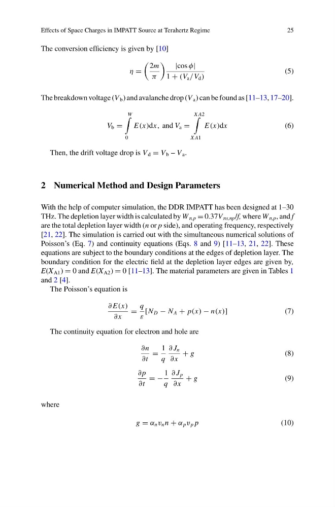
The conversion efficiency is given by [10]
η =
2m
π
|cos φ|
1 + (V a /V d )
(5)
The breakdown voltage (V b ) and avalanche drop (V a ) can be found as [11–13, 17–20].
V b =
W
0
E(x)dx, and V a =
X A2
X A1
E(x)dx
(6)
Then, the drift voltage drop is V d = V b – V a .
2 Numerical Method and Design Parameters
With the help of computer simulation, the DDR IMPATT has been designed at 1–30
THz. The depletion layer width is calculated by W n,p = 0.37V ns,np /f, where W n,p , and f
are the total depletion layer width (n or p side), and operating frequency, respectively
[21, 22]. The simulation is carried out with the simultaneous numerical solutions of
Poisson’s (Eq. 7) and continuity equations (Eqs. 8 and 9) [11–13, 21, 22]. These
equations are subject to the boundary conditions at the edges of depletion layer. The
boundary condition for the electric field at the depletion layer edges are given by,
E(X A1 ) = 0 and E(X A2 ) = 0 [11–13]. The material parameters are given in Tables 1
and 2 [4].
The Poisson’s equation is
∂ E(x)
∂ x
=
q
ε
[N D − N A + p(x) − n(x)]
(7)
The continuity equation for electron and hole are
∂n
∂t
=
1
q
∂ J n
∂ x
+ g
(8)
∂ p
∂t
= −
1
q
∂ J p
∂ x
+ g
(9)
where
g = α n v n n + α p v p p
(10)
25
The conversion efficiency is given by [10]
η =
2m
π
|cos φ|
1 + (V a /V d )
(5)
The breakdown voltage (V b ) and avalanche drop (V a ) can be found as [11–13, 17–20].
V b =
W
0
E(x)dx, and V a =
X A2
X A1
E(x)dx
(6)
Then, the drift voltage drop is V d = V b – V a .
2 Numerical Method and Design Parameters
With the help of computer simulation, the DDR IMPATT has been designed at 1–30
THz. The depletion layer width is calculated by W n,p = 0.37V ns,np /f, where W n,p , and f
are the total depletion layer width (n or p side), and operating frequency, respectively
[21, 22]. The simulation is carried out with the simultaneous numerical solutions of
Poisson’s (Eq. 7) and continuity equations (Eqs. 8 and 9) [11–13, 21, 22]. These
equations are subject to the boundary conditions at the edges of depletion layer. The
boundary condition for the electric field at the depletion layer edges are given by,
E(X A1 ) = 0 and E(X A2 ) = 0 [11–13]. The material parameters are given in Tables 1
and 2 [4].
The Poisson’s equation is
∂ E(x)
∂ x
=
q
ε
[N D − N A + p(x) − n(x)]
(7)
The continuity equation for electron and hole are
∂n
∂t
=
1
q
∂ J n
∂ x
+ g
(8)
∂ p
∂t
= −
1
q
∂ J p
∂ x
+ g
(9)
where
g = α n v n n + α p v p p
(10)