

214
R. Singh et al.
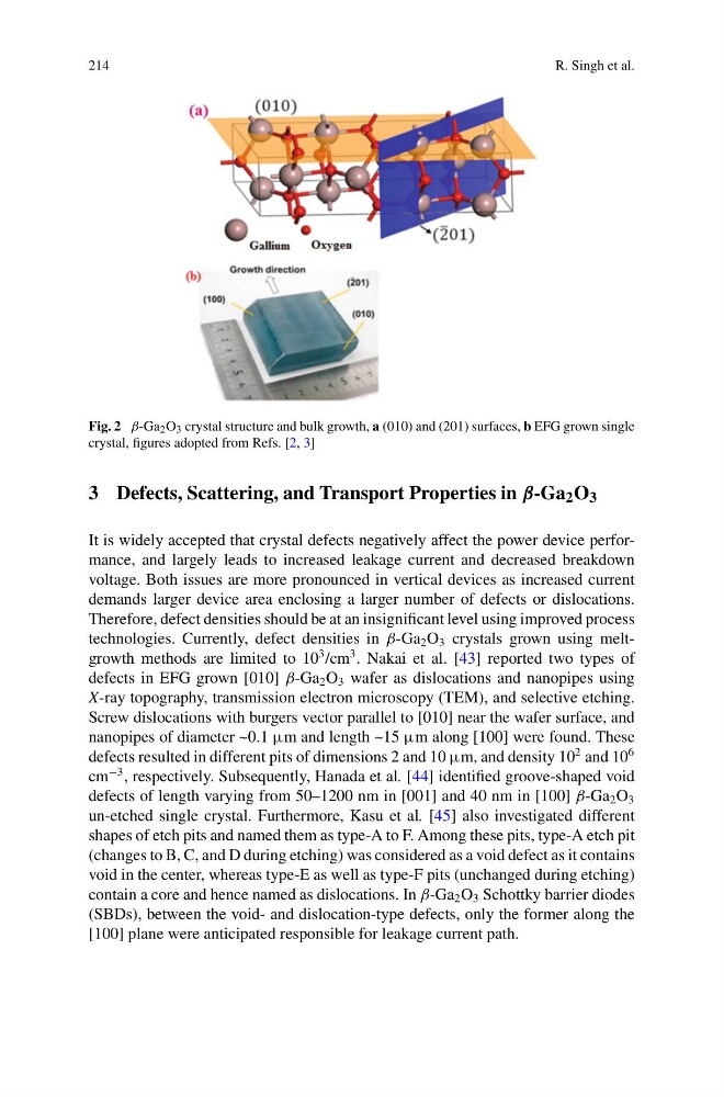
Fig. 2 β-Ga 2 O 3 crystal structure and bulk growth, a (010) and (201) surfaces, b EFG grown single
crystal, figures adopted from Refs. [2, 3]
3 Defects, Scattering, and Transport Properties in β-Ga 2 O 3
It is widely accepted that crystal defects negatively affect the power device performance, and largely leads to increased leakage current and decreased breakdown
voltage. Both issues are more pronounced in vertical devices as increased current
demands larger device area enclosing a larger number of defects or dislocations.
Therefore, defect densities should be at an insignificant level using improved process
technologies. Currently, defect densities in β-Ga 2 O 3 crystals grown using meltgrowth methods are limited to 10
3 /cm
3 . Nakai et al. [43] reported two types of
defects in EFG grown [010] β-Ga 2 O 3 wafer as dislocations and nanopipes using
X-ray topography, transmission electron microscopy (TEM), and selective etching.
Screw dislocations with burgers vector parallel to [010] near the wafer surface, and
nanopipes of diameter ~0.1 μm and length ~15 μm along [100] were found. These
defects resulted in different pits of dimensions 2 and 10 μm, and density 10
2 and 10
6
cm
−3 , respectively. Subsequently, Hanada et al. [44] identified groove-shaped void
defects of length varying from 50–1200 nm in [001] and 40 nm in [100] β-Ga 2 O 3
un-etched single crystal. Furthermore, Kasu et al. [45] also investigated different
shapes of etch pits and named them as type-A to F. Among these pits, type-A etch pit
(changes to B, C, and D during etching) was considered as a void defect as it contains
void in the center, whereas type-E as well as type-F pits (unchanged during etching)
contain a core and hence named as dislocations. In β-Ga 2 O 3 Schottky barrier diodes
(SBDs), between the void- and dislocation-type defects, only the former along the
[100] plane were anticipated responsible for leakage current path.
R. Singh et al.
Fig. 2 β-Ga 2 O 3 crystal structure and bulk growth, a (010) and (201) surfaces, b EFG grown single
crystal, figures adopted from Refs. [2, 3]
3 Defects, Scattering, and Transport Properties in β-Ga 2 O 3
It is widely accepted that crystal defects negatively affect the power device performance, and largely leads to increased leakage current and decreased breakdown
voltage. Both issues are more pronounced in vertical devices as increased current
demands larger device area enclosing a larger number of defects or dislocations.
Therefore, defect densities should be at an insignificant level using improved process
technologies. Currently, defect densities in β-Ga 2 O 3 crystals grown using meltgrowth methods are limited to 10
3 /cm
3 . Nakai et al. [43] reported two types of
defects in EFG grown [010] β-Ga 2 O 3 wafer as dislocations and nanopipes using
X-ray topography, transmission electron microscopy (TEM), and selective etching.
Screw dislocations with burgers vector parallel to [010] near the wafer surface, and
nanopipes of diameter ~0.1 μm and length ~15 μm along [100] were found. These
defects resulted in different pits of dimensions 2 and 10 μm, and density 10
2 and 10
6
cm
−3 , respectively. Subsequently, Hanada et al. [44] identified groove-shaped void
defects of length varying from 50–1200 nm in [001] and 40 nm in [100] β-Ga 2 O 3
un-etched single crystal. Furthermore, Kasu et al. [45] also investigated different
shapes of etch pits and named them as type-A to F. Among these pits, type-A etch pit
(changes to B, C, and D during etching) was considered as a void defect as it contains
void in the center, whereas type-E as well as type-F pits (unchanged during etching)
contain a core and hence named as dislocations. In β-Ga 2 O 3 Schottky barrier diodes
(SBDs), between the void- and dislocation-type defects, only the former along the
[100] plane were anticipated responsible for leakage current path.