

Ga 2 O 3 Based Heterostructure FETs (HFETs) for Microwave …
213
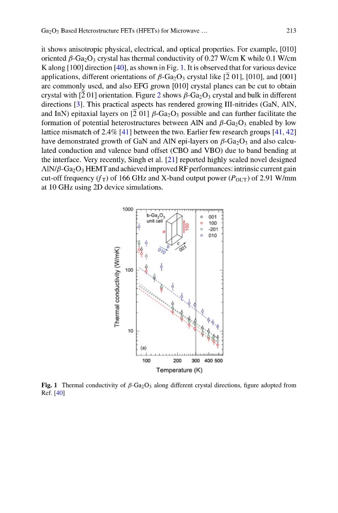
it shows anisotropic physical, electrical, and optical properties. For example, [010]
oriented β-Ga 2 O 3 crystal has thermal conductivity of 0.27 W/cm K while 0.1 W/cm
K along [100] direction [40], as shown in Fig. 1. It is observed that for various device
applications, different orientations of β-Ga 2 O 3 crystal like [2 01], [010], and [001]
are commonly used, and also EFG grown [010] crystal planes can be cut to obtain
crystal with [2 01] orientation. Figure 2 shows β-Ga 2 O 3 crystal and bulk in different
directions [3]. This practical aspects has rendered growing III-nitrides (GaN, AlN,
and InN) epitaxial layers on [2 01] β-Ga 2 O 3 possible and can further facilitate the
formation of potential heterostructures between AlN and β-Ga 2 O 3 enabled by low
lattice mismatch of 2.4% [41] between the two. Earlier few research groups [41, 42]
have demonstrated growth of GaN and AlN epi-layers on β-Ga 2 O 3 and also calculated conduction and valence band offset (CBO and VBO) due to band bending at
the interface. Very recently, Singh et al. [21] reported highly scaled novel designed
AlN/β-Ga 2 O 3 HEMT and achieved improved RF performances: intrinsic current gain
cut-off frequency (f T ) of 166 GHz and X-band output power (P OUT ) of 2.91 W/mm
at 10 GHz using 2D device simulations.
Fig. 1 Thermal conductivity of β-Ga 2 O 3 along different crystal directions, figure adopted from
Ref. [40]
213
it shows anisotropic physical, electrical, and optical properties. For example, [010]
oriented β-Ga 2 O 3 crystal has thermal conductivity of 0.27 W/cm K while 0.1 W/cm
K along [100] direction [40], as shown in Fig. 1. It is observed that for various device
applications, different orientations of β-Ga 2 O 3 crystal like [2 01], [010], and [001]
are commonly used, and also EFG grown [010] crystal planes can be cut to obtain
crystal with [2 01] orientation. Figure 2 shows β-Ga 2 O 3 crystal and bulk in different
directions [3]. This practical aspects has rendered growing III-nitrides (GaN, AlN,
and InN) epitaxial layers on [2 01] β-Ga 2 O 3 possible and can further facilitate the
formation of potential heterostructures between AlN and β-Ga 2 O 3 enabled by low
lattice mismatch of 2.4% [41] between the two. Earlier few research groups [41, 42]
have demonstrated growth of GaN and AlN epi-layers on β-Ga 2 O 3 and also calculated conduction and valence band offset (CBO and VBO) due to band bending at
the interface. Very recently, Singh et al. [21] reported highly scaled novel designed
AlN/β-Ga 2 O 3 HEMT and achieved improved RF performances: intrinsic current gain
cut-off frequency (f T ) of 166 GHz and X-band output power (P OUT ) of 2.91 W/mm
at 10 GHz using 2D device simulations.
Fig. 1 Thermal conductivity of β-Ga 2 O 3 along different crystal directions, figure adopted from
Ref. [40]