

All Optical Universal Logic TAND Gate Using a Single …
175
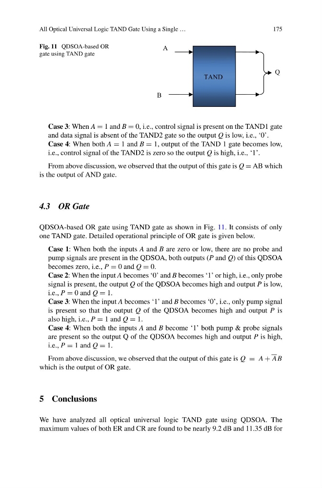
Fig. 11 QDSOA-based OR
gate using TAND gate
TAND
B
Q
A
Case 3: When A = 1 and B = 0, i.e., control signal is present on the TAND1 gate
and data signal is absent of the TAND2 gate so the output Q is low, i.e., ‘0’.
Case 4: When both A = 1 and B = 1, output of the TAND 1 gate becomes low,
i.e., control signal of the TAND2 is zero so the output Q is high, i.e., ‘1’.
From above discussion, we observed that the output of this gate is Q = AB which
is the output of AND gate.
4.3 OR Gate
QDSOA-based OR gate using TAND gate as shown in Fig. 11. It consists of only
one TAND gate. Detailed operational principle of OR gate is given below.
Case 1: When both the inputs A and B are zero or low, there are no probe and
pump signals are present in the QDSOA, both outputs (P and Q) of this QDSOA
becomes zero, i.e., P = 0 and Q = 0.
Case 2: When the input A becomes ‘0’ and B becomes ‘1’ or high, i.e., only probe
signal is present, the output Q of the QDSOA becomes high and output P is low,
i.e., P = 0 and Q = 1.
Case 3: When the input A becomes ‘1’ and B becomes ‘0’, i.e., only pump signal
is present so that the output Q of the QDSOA becomes high and output P is
also high, i.e., P = 1 and Q = 1.
Case 4: When both the inputs A and B become ‘1’ both pump & probe signals
are present so the output Q of the QDSOA becomes high and output P is high,
i.e., P = 1 and Q = 1.
From above discussion, we observed that the output of this gate is Q = A + AB
which is the output of OR gate.
5 Conclusions
We have analyzed all optical universal logic TAND gate using QDSOA. The
maximum values of both ER and CR are found to be nearly 9.2 dB and 11.35 dB for
175
Fig. 11 QDSOA-based OR
gate using TAND gate
TAND
B
Q
A
Case 3: When A = 1 and B = 0, i.e., control signal is present on the TAND1 gate
and data signal is absent of the TAND2 gate so the output Q is low, i.e., ‘0’.
Case 4: When both A = 1 and B = 1, output of the TAND 1 gate becomes low,
i.e., control signal of the TAND2 is zero so the output Q is high, i.e., ‘1’.
From above discussion, we observed that the output of this gate is Q = AB which
is the output of AND gate.
4.3 OR Gate
QDSOA-based OR gate using TAND gate as shown in Fig. 11. It consists of only
one TAND gate. Detailed operational principle of OR gate is given below.
Case 1: When both the inputs A and B are zero or low, there are no probe and
pump signals are present in the QDSOA, both outputs (P and Q) of this QDSOA
becomes zero, i.e., P = 0 and Q = 0.
Case 2: When the input A becomes ‘0’ and B becomes ‘1’ or high, i.e., only probe
signal is present, the output Q of the QDSOA becomes high and output P is low,
i.e., P = 0 and Q = 1.
Case 3: When the input A becomes ‘1’ and B becomes ‘0’, i.e., only pump signal
is present so that the output Q of the QDSOA becomes high and output P is
also high, i.e., P = 1 and Q = 1.
Case 4: When both the inputs A and B become ‘1’ both pump & probe signals
are present so the output Q of the QDSOA becomes high and output P is high,
i.e., P = 1 and Q = 1.
From above discussion, we observed that the output of this gate is Q = A + AB
which is the output of OR gate.
5 Conclusions
We have analyzed all optical universal logic TAND gate using QDSOA. The
maximum values of both ER and CR are found to be nearly 9.2 dB and 11.35 dB for