

A Novel Integrated Power Module with Solid-State …
7
2.3 IMPATT Diode
IMPATT (IMPact Avalanche Transit Time) is a reverse-biased junction diode that
exhibits negative resistance due to 180° to 270° phase difference between the applied
bias voltage and the generated RF current [14]. It has an ‘avalanche region’, where
electron shower, i.e. avalnce of electrons, is generated due to high-field effect at a p
+ n
junction (the avalanche process is an inductive process), and a ‘drift region’/‘transittime region’ where more than 90° phase difference is produced between the voltage
being applied and the current being generated. When the predominantly capacitance
impedance of the diode is resonated with the inductive impedance of an RF cavity (in
which the diode is embedded), RF oscillation is obtained at microwave or millimetrewave frequency depending on the diode design parameters and cavity dimensions.
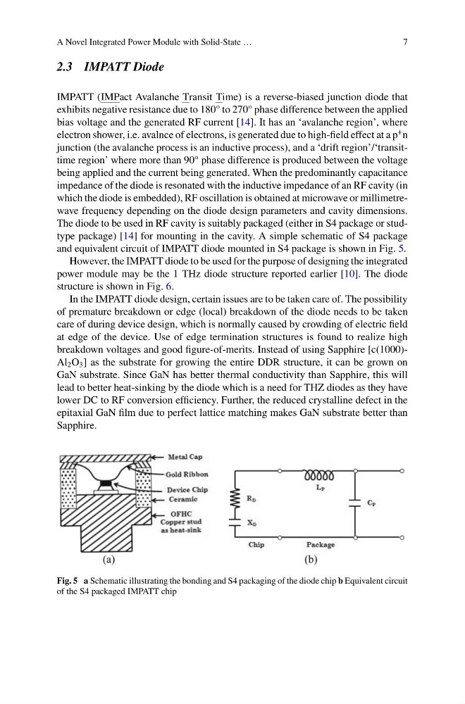
The diode to be used in RF cavity is suitably packaged (either in S4 package or studtype package) [14] for mounting in the cavity. A simple schematic of S4 package
and equivalent circuit of IMPATT diode mounted in S4 package is shown in Fig. 5.
However, the IMPATT diode to be used for the purpose of designing the integrated
power module may be the 1 THz diode structure reported earlier [10]. The diode
structure is shown in Fig. 6.
In the IMPATT diode design, certain issues are to be taken care of. The possibility
of premature breakdown or edge (local) breakdown of the diode needs to be taken
care of during device design, which is normally caused by crowding of electric field
at edge of the device. Use of edge termination structures is found to realize high
breakdown voltages and good figure-of-merits. Instead of using Sapphire [c(1000)Al 2 O 3 ] as the substrate for growing the entire DDR structure, it can be grown on
GaN substrate. Since GaN has better thermal conductivity than Sapphire, this will
lead to better heat-sinking by the diode which is a need for THZ diodes as they have
lower DC to RF conversion efficiency. Further, the reduced crystalline defect in the
epitaxial GaN film due to perfect lattice matching makes GaN substrate better than
Sapphire.
Fig. 5 a Schematic illustrating the bonding and S4 packaging of the diode chip b Equivalent circuit
of the S4 packaged IMPATT chip
7
2.3 IMPATT Diode
IMPATT (IMPact Avalanche Transit Time) is a reverse-biased junction diode that
exhibits negative resistance due to 180° to 270° phase difference between the applied
bias voltage and the generated RF current [14]. It has an ‘avalanche region’, where
electron shower, i.e. avalnce of electrons, is generated due to high-field effect at a p
+ n
junction (the avalanche process is an inductive process), and a ‘drift region’/‘transittime region’ where more than 90° phase difference is produced between the voltage
being applied and the current being generated. When the predominantly capacitance
impedance of the diode is resonated with the inductive impedance of an RF cavity (in
which the diode is embedded), RF oscillation is obtained at microwave or millimetrewave frequency depending on the diode design parameters and cavity dimensions.
The diode to be used in RF cavity is suitably packaged (either in S4 package or studtype package) [14] for mounting in the cavity. A simple schematic of S4 package
and equivalent circuit of IMPATT diode mounted in S4 package is shown in Fig. 5.
However, the IMPATT diode to be used for the purpose of designing the integrated
power module may be the 1 THz diode structure reported earlier [10]. The diode
structure is shown in Fig. 6.
In the IMPATT diode design, certain issues are to be taken care of. The possibility
of premature breakdown or edge (local) breakdown of the diode needs to be taken
care of during device design, which is normally caused by crowding of electric field
at edge of the device. Use of edge termination structures is found to realize high
breakdown voltages and good figure-of-merits. Instead of using Sapphire [c(1000)Al 2 O 3 ] as the substrate for growing the entire DDR structure, it can be grown on
GaN substrate. Since GaN has better thermal conductivity than Sapphire, this will
lead to better heat-sinking by the diode which is a need for THZ diodes as they have
lower DC to RF conversion efficiency. Further, the reduced crystalline defect in the
epitaxial GaN film due to perfect lattice matching makes GaN substrate better than
Sapphire.
Fig. 5 a Schematic illustrating the bonding and S4 packaging of the diode chip b Equivalent circuit
of the S4 packaged IMPATT chip