

6
S. Kar
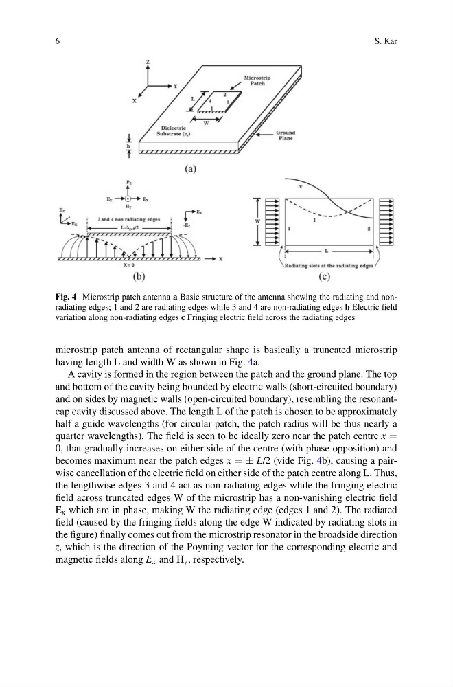
Fig. 4 Microstrip patch antenna a Basic structure of the antenna showing the radiating and nonradiating edges; 1 and 2 are radiating edges while 3 and 4 are non-radiating edges b Electric field
variation along non-radiating edges c Fringing electric field across the radiating edges
microstrip patch antenna of rectangular shape is basically a truncated microstrip
having length L and width W as shown in Fig. 4a.
A cavity is formed in the region between the patch and the ground plane. The top
and bottom of the cavity being bounded by electric walls (short-circuited boundary)
and on sides by magnetic walls (open-circuited boundary), resembling the resonantcap cavity discussed above. The length L of the patch is chosen to be approximately
half a guide wavelengths (for circular patch, the patch radius will be thus nearly a
quarter wavelengths). The field is seen to be ideally zero near the patch centre x =
0, that gradually increases on either side of the centre (with phase opposition) and
becomes maximum near the patch edges x = ± L/2 (vide Fig. 4b), causing a pairwise cancellation of the electric field on either side of the patch centre along L. Thus,
the lengthwise edges 3 and 4 act as non-radiating edges while the fringing electric
field across truncated edges W of the microstrip has a non-vanishing electric field
E x which are in phase, making W the radiating edge (edges 1 and 2). The radiated
field (caused by the fringing fields along the edge W indicated by radiating slots in
the figure) finally comes out from the microstrip resonator in the broadside direction
z, which is the direction of the Poynting vector for the corresponding electric and
magnetic fields along E x and H y , respectively.
S. Kar
Fig. 4 Microstrip patch antenna a Basic structure of the antenna showing the radiating and nonradiating edges; 1 and 2 are radiating edges while 3 and 4 are non-radiating edges b Electric field
variation along non-radiating edges c Fringing electric field across the radiating edges
microstrip patch antenna of rectangular shape is basically a truncated microstrip
having length L and width W as shown in Fig. 4a.
A cavity is formed in the region between the patch and the ground plane. The top
and bottom of the cavity being bounded by electric walls (short-circuited boundary)
and on sides by magnetic walls (open-circuited boundary), resembling the resonantcap cavity discussed above. The length L of the patch is chosen to be approximately
half a guide wavelengths (for circular patch, the patch radius will be thus nearly a
quarter wavelengths). The field is seen to be ideally zero near the patch centre x =
0, that gradually increases on either side of the centre (with phase opposition) and
becomes maximum near the patch edges x = ± L/2 (vide Fig. 4b), causing a pairwise cancellation of the electric field on either side of the patch centre along L. Thus,
the lengthwise edges 3 and 4 act as non-radiating edges while the fringing electric
field across truncated edges W of the microstrip has a non-vanishing electric field
E x which are in phase, making W the radiating edge (edges 1 and 2). The radiated
field (caused by the fringing fields along the edge W indicated by radiating slots in
the figure) finally comes out from the microstrip resonator in the broadside direction
z, which is the direction of the Poynting vector for the corresponding electric and
magnetic fields along E x and H y , respectively.