

200
M. Mochizuki
Table 8.2 Typical material parameters for magnetic bilayer systems
Metallic systems
Semiconducting systems
Lattice constant a
5 Å
5 Å
Fermi energy E F
4 eV
10 meV
Fermi wavenumber k F
1 Å −1
0.01 Å −1
Exchange int. J ex /E F
0.25
0.5
Relaxation time τ
10 −14 s
10 −12 s
Rashba parameter 1: α 0
2 eV·Å
0.07 eV·Å
Rashba parameter 2: α ext /α 0
0.1
0.1
Frequency /2π
1 GHz
1 GHz
(Note that m × (a
2
/)δH DMI /δm leads to T 1 + T 2 ). The contribution D 1 , which is
proportional to α R , appears even with a steady Rashba spin-orbit interaction. In contrast, the contribution D 2 , which is proportional to ∂ t α R , appears only in the presence
of a time-dependent Rashba spin-orbit interaction. This interfacial DzyaloshinskiiMoriya interaction is expected to be tuned by applying an electric gate voltage. More
interestingly, application of an AC voltage is expected to induce an oscillating component of the Dzyaloshinskii-Moriya interaction. The Rashba parameter α R (t) in the
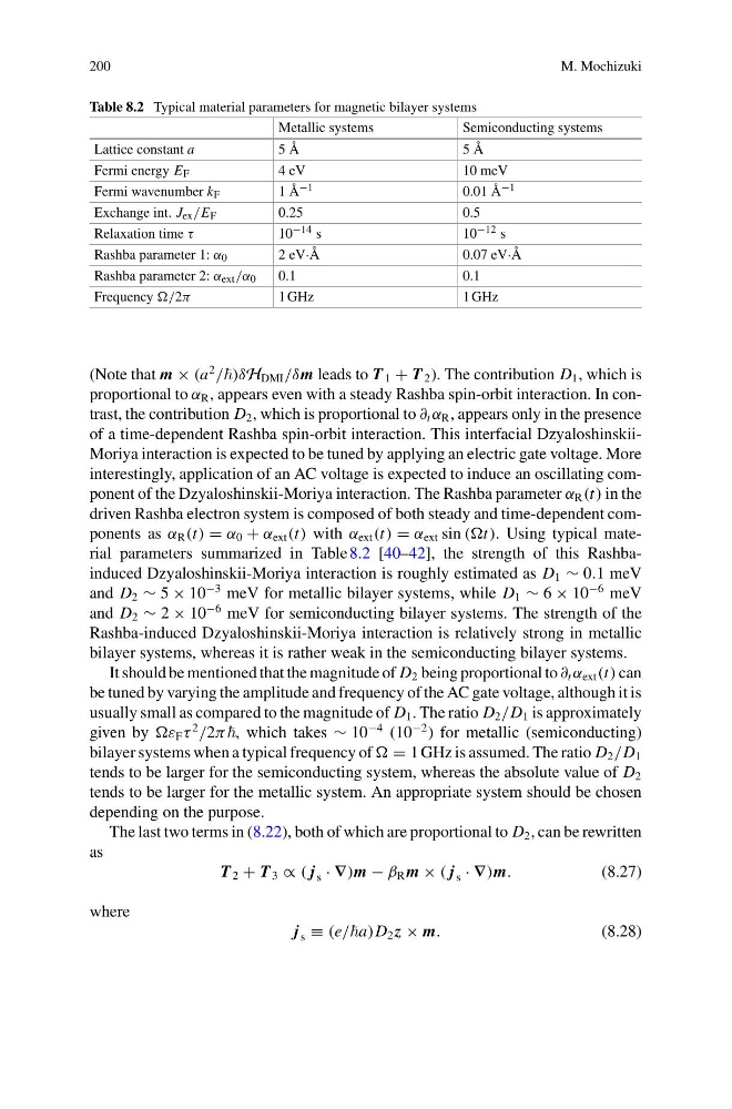
driven Rashba electron system is composed of both steady and time-dependent components as α R (t) = α 0 + α ext (t) with α ext (t) = α ext sin ((t). Using typical material parameters summarized in Table 8.2 [40–42], the strength of this Rashbainduced Dzyaloshinskii-Moriya interaction is roughly estimated as D 1 ∼ 0.1 meV
and D 2 ∼ 5 × 10
−3 meV for metallic bilayer systems, while D 1 ∼ 6 × 10
−6 meV
and D 2 ∼ 2 × 10
−6 meV for semiconducting bilayer systems. The strength of the
Rashba-induced Dzyaloshinskii-Moriya interaction is relatively strong in metallic
bilayer systems, whereas it is rather weak in the semiconducting bilayer systems.
It should be mentioned that the magnitude of D 2 being proportional to ∂ t α ext (t) can
be tuned by varying the amplitude and frequency of the AC gate voltage, although it is
usually small as compared to the magnitude of D 1 . The ratio D 2 /D 1 is approximately
given by ε F τ
2
/2π , which takes ∼ 10
−4 (10
−2 ) for metallic (semiconducting)
bilayer systems when a typical frequency of = 1 GHz is assumed. The ratio D 2 /D 1
tends to be larger for the semiconducting system, whereas the absolute value of D 2
tends to be larger for the metallic system. An appropriate system should be chosen
depending on the purpose.
The last two terms in (8.22), both of which are proportional to D 2 , can be rewritten
as
T 2 + T 3 ∝ ( j s · ∇)m − β R m × ( j s · ∇)m.
(8.27)
where
j s ≡ (e/a)D 2 z × m.
(8.28)
M. Mochizuki
Table 8.2 Typical material parameters for magnetic bilayer systems
Metallic systems
Semiconducting systems
Lattice constant a
5 Å
5 Å
Fermi energy E F
4 eV
10 meV
Fermi wavenumber k F
1 Å −1
0.01 Å −1
Exchange int. J ex /E F
0.25
0.5
Relaxation time τ
10 −14 s
10 −12 s
Rashba parameter 1: α 0
2 eV·Å
0.07 eV·Å
Rashba parameter 2: α ext /α 0
0.1
0.1
Frequency /2π
1 GHz
1 GHz
(Note that m × (a
2
/)δH DMI /δm leads to T 1 + T 2 ). The contribution D 1 , which is
proportional to α R , appears even with a steady Rashba spin-orbit interaction. In contrast, the contribution D 2 , which is proportional to ∂ t α R , appears only in the presence
of a time-dependent Rashba spin-orbit interaction. This interfacial DzyaloshinskiiMoriya interaction is expected to be tuned by applying an electric gate voltage. More
interestingly, application of an AC voltage is expected to induce an oscillating component of the Dzyaloshinskii-Moriya interaction. The Rashba parameter α R (t) in the
driven Rashba electron system is composed of both steady and time-dependent components as α R (t) = α 0 + α ext (t) with α ext (t) = α ext sin ((t). Using typical material parameters summarized in Table 8.2 [40–42], the strength of this Rashbainduced Dzyaloshinskii-Moriya interaction is roughly estimated as D 1 ∼ 0.1 meV
and D 2 ∼ 5 × 10
−3 meV for metallic bilayer systems, while D 1 ∼ 6 × 10
−6 meV
and D 2 ∼ 2 × 10
−6 meV for semiconducting bilayer systems. The strength of the
Rashba-induced Dzyaloshinskii-Moriya interaction is relatively strong in metallic
bilayer systems, whereas it is rather weak in the semiconducting bilayer systems.
It should be mentioned that the magnitude of D 2 being proportional to ∂ t α ext (t) can
be tuned by varying the amplitude and frequency of the AC gate voltage, although it is
usually small as compared to the magnitude of D 1 . The ratio D 2 /D 1 is approximately
given by ε F τ
2
/2π , which takes ∼ 10
−4 (10
−2 ) for metallic (semiconducting)
bilayer systems when a typical frequency of = 1 GHz is assumed. The ratio D 2 /D 1
tends to be larger for the semiconducting system, whereas the absolute value of D 2
tends to be larger for the metallic system. An appropriate system should be chosen
depending on the purpose.
The last two terms in (8.22), both of which are proportional to D 2 , can be rewritten
as
T 2 + T 3 ∝ ( j s · ∇)m − β R m × ( j s · ∇)m.
(8.27)
where
j s ≡ (e/a)D 2 z × m.
(8.28)