

C hapter 10 nanomaterial product Forms and Functions
432
embedded in many bulk polymer materials. Bulk forms were discussed in previous chapters and include many kinds of nanometals,
nanopolymers, and nanoceramics (Section 8.8). We have also seen
that nanocomposites can take several primary physical forms, such
as nanoparticles or nanotubes embedded in a matrix, or films or
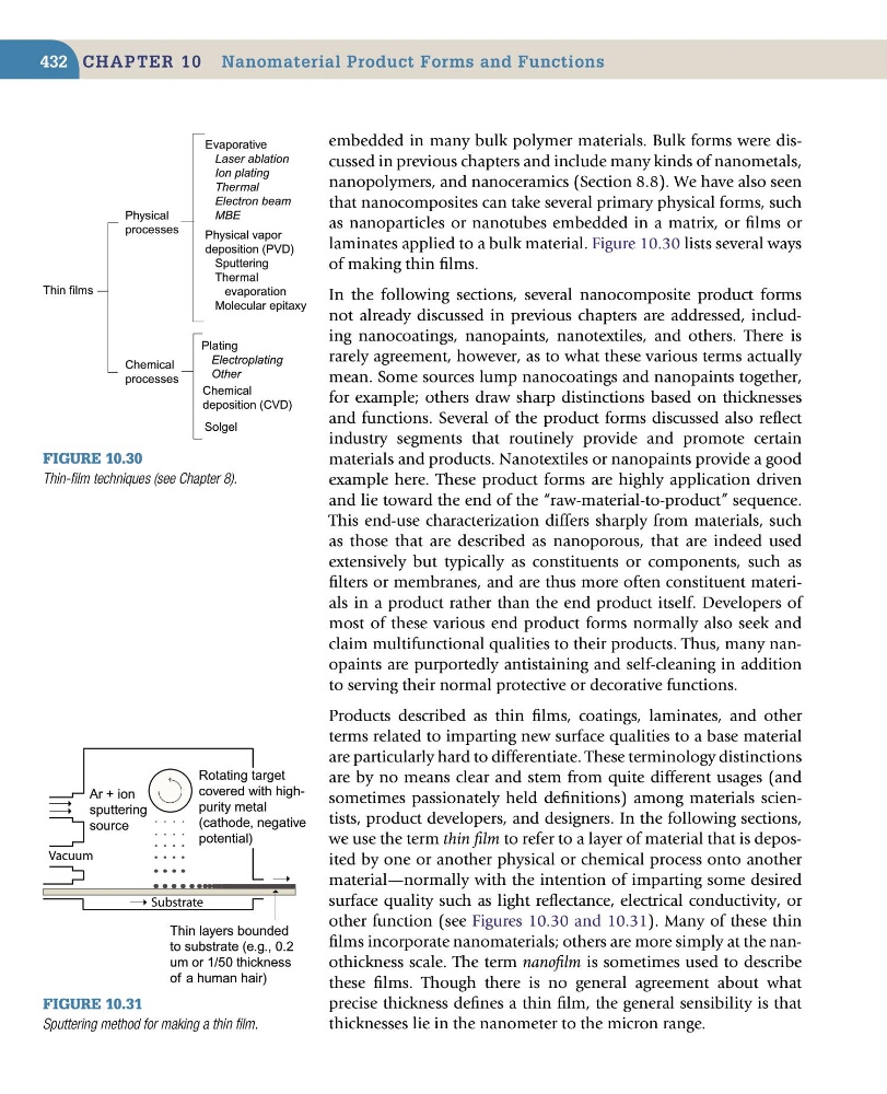
laminates applied to a bulk material. Figure 10.30 lists several ways
of making thin films.
In the following sections, several nanocomposite product forms
not already discussed in previous chapters are addressed, including nanocoatings, nanopaints, nanotextiles, and others. There is
rarely agreement, however, as to what these various terms actually
mean. Some sources lump nanocoatings and nanopaints together,
for example; others draw sharp distinctions based on thicknesses
and functions. Several of the product forms discussed also reflect
industry segments that routinely provide and promote certain
materials and products. Nanotextiles or nanopaints provide a good
example here. These product forms are highly application driven
and lie toward the end of the “raw-material-to-product” sequence.
This end-use characterization differs sharply from materials, such
as those that are described as nanoporous, that are indeed used
extensively but typically as constituents or components, such as
filters or membranes, and are thus more often constituent materials in a product rather than the end product itself. Developers of
most of these various end product forms normally also seek and
claim multifunctional qualities to their products. Thus, many nanopaints are purportedly antistaining and self-cleaning in addition
to serving their normal protective or decorative functions.
Products described as thin films, coatings, laminates, and other
terms related to imparting new surface qualities to a base material
are particularly hard to differentiate. These terminology distinctions
are by no means clear and stem from quite different usages (and
sometimes passionately held definitions) among materials scientists, product developers, and designers. In the following sections,
we use the term thin film to refer to a layer of material that is deposited by one or another physical or chemical process onto another
material—normally with the intention of imparting some desired
surface quality such as light reflectance, electrical conductivity, or
other function (see Figures 10.30 and 10.31). Many of these thin
films incorporate nanomaterials; others are more simply at the nanothickness scale. The term nanofilm is sometimes used to describe
these films. Though there is no general agreement about what
precise thickness defines a thin film, the general sensibility is that
thicknesses lie in the nanometer to the micron range.
Figure 10.30
Thin-film techniques (see Chapter 8).
Thin films
Physical
processes
Chemical
processes
Evaporative
Laser ablation
Ion plating
Thermal
Electron beam
MBE
Physical vapor
deposition (PVD)
Sputtering
Thermal
evaporation
Molecular epitaxy
Solgel
Plating
Electroplating
Other
Chemical
deposition (CVD)
Figure 10.31
Sputtering method for making a thin film.
Rotating target
covered with highpurity metal
(cathode, negative
potential)
Vacuum
Substrate
Ar + ion
sputtering
source
Thin layers bounded
to substrate (e.g., 0.2
um or 1/50 thickness
of a human hair)
432
embedded in many bulk polymer materials. Bulk forms were discussed in previous chapters and include many kinds of nanometals,
nanopolymers, and nanoceramics (Section 8.8). We have also seen
that nanocomposites can take several primary physical forms, such
as nanoparticles or nanotubes embedded in a matrix, or films or
laminates applied to a bulk material. Figure 10.30 lists several ways
of making thin films.
In the following sections, several nanocomposite product forms
not already discussed in previous chapters are addressed, including nanocoatings, nanopaints, nanotextiles, and others. There is
rarely agreement, however, as to what these various terms actually
mean. Some sources lump nanocoatings and nanopaints together,
for example; others draw sharp distinctions based on thicknesses
and functions. Several of the product forms discussed also reflect
industry segments that routinely provide and promote certain
materials and products. Nanotextiles or nanopaints provide a good
example here. These product forms are highly application driven
and lie toward the end of the “raw-material-to-product” sequence.
This end-use characterization differs sharply from materials, such
as those that are described as nanoporous, that are indeed used
extensively but typically as constituents or components, such as
filters or membranes, and are thus more often constituent materials in a product rather than the end product itself. Developers of
most of these various end product forms normally also seek and
claim multifunctional qualities to their products. Thus, many nanopaints are purportedly antistaining and self-cleaning in addition
to serving their normal protective or decorative functions.
Products described as thin films, coatings, laminates, and other
terms related to imparting new surface qualities to a base material
are particularly hard to differentiate. These terminology distinctions
are by no means clear and stem from quite different usages (and
sometimes passionately held definitions) among materials scientists, product developers, and designers. In the following sections,
we use the term thin film to refer to a layer of material that is deposited by one or another physical or chemical process onto another
material—normally with the intention of imparting some desired
surface quality such as light reflectance, electrical conductivity, or
other function (see Figures 10.30 and 10.31). Many of these thin
films incorporate nanomaterials; others are more simply at the nanothickness scale. The term nanofilm is sometimes used to describe
these films. Though there is no general agreement about what
precise thickness defines a thin film, the general sensibility is that
thicknesses lie in the nanometer to the micron range.
Figure 10.30
Thin-film techniques (see Chapter 8).
Thin films
Physical
processes
Chemical
processes
Evaporative
Laser ablation
Ion plating
Thermal
Electron beam
MBE
Physical vapor
deposition (PVD)
Sputtering
Thermal
evaporation
Molecular epitaxy
Solgel
Plating
Electroplating
Other
Chemical
deposition (CVD)
Figure 10.31
Sputtering method for making a thin film.
Rotating target
covered with highpurity metal
(cathode, negative
potential)
Vacuum
Substrate
Ar + ion
sputtering
source
Thin layers bounded
to substrate (e.g., 0.2
um or 1/50 thickness
of a human hair)