

chapter 8 nanomaterials: Synthesis and characterization
284
surface topography are obtained by monitoring the deflection of
the cantilever. In this mode, the scanning speed is slow due to the
response of the feedback system, but the force on the sample is
well controlled. However, the large friction forces can damage the
sample. Still, this is the preferred mode used for most applications.
A different method of operation is the taping mode. In this case,
the tip is oscillated at the beam’s natural frequency so that the tip
contacts the sample, tapping it but not dragging across it, thereby
reducing the possibility of damaging the sample. It is a compromise between contact and noncontact AFM. The topography of the
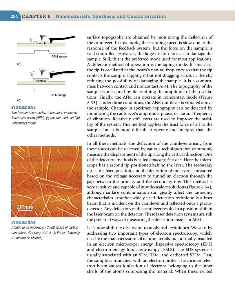
sample is measured by determining the amplitude of the oscillations. Finally, the AFM can operate in noncontact mode (Figure
8.53). Under these conditions, the AFM cantilever is vibrated above
the sample. Changes in specimen topography can be detected by
monitoring the cantilever’s amplitude, phase, or natural frequency
of vibration. Relatively stiff levers are used to improve the stability of the system. This method applies the least force of all to the
sample, but it is more difficult to operate and interpret than the
other methods.
In all these methods, the deflection of the cantilever arising from
these forces can be detected by various techniques that commonly
measure the displacement of the tip along the vertical direction. One
of the detection methods is called tunneling detection. Here the microscope has a second tip positioned behind the lever. The secondary
tip is in a fixed position, and the deflection of the lever is measured
based on the voltage necessary to tunnel an electron through the
gap between the primary and the secondary tips. This method is
very sensitive and capable of atomic-scale resolutions (Figure 8.54),
although surface contamination can greatly affect the tunneling
characteristics. Another widely used detection technique is a laser
beam that is incident on the cantilever and reflected onto a photodetector. Any deflection of the cantilever results in a position shift of
the laser beam on the detector. These laser detection systems are still
the preferred ways of measuring the deflection inside an AFM.
Let’s now shift the discussion to analytical techniques. We start by
addressing two important types of electron spectroscopy, widely
used in the characterization of nanomaterials and normally installed
in an electron microscope: energy dispersive spectroscopy (EDS)
and electron energy loss spectroscopy (EELS). The EDS system is
usually associated with an SEM, TEM, and dedicated STEM. First,
the sample is irradiated with an electron probe. The incident electron beam causes ionization of electrons belonging to the inner
shells of the atoms composing the material. When these excited
Figure 8.53
The two common modes of operation in atomic
force microscopy (AFM): (a) contact mode and (b)
noncontact mode.
AFM image
AFM image
(a)
(b)
Sample
Sample
Figure 8.54
Atomic force microscopy (AFM) image of carbon
nanotubes. (Courtesy of P. J. de Pablo, University
Autonoma de Madrid.)
284
surface topography are obtained by monitoring the deflection of
the cantilever. In this mode, the scanning speed is slow due to the
response of the feedback system, but the force on the sample is
well controlled. However, the large friction forces can damage the
sample. Still, this is the preferred mode used for most applications.
A different method of operation is the taping mode. In this case,
the tip is oscillated at the beam’s natural frequency so that the tip
contacts the sample, tapping it but not dragging across it, thereby
reducing the possibility of damaging the sample. It is a compromise between contact and noncontact AFM. The topography of the
sample is measured by determining the amplitude of the oscillations. Finally, the AFM can operate in noncontact mode (Figure
8.53). Under these conditions, the AFM cantilever is vibrated above
the sample. Changes in specimen topography can be detected by
monitoring the cantilever’s amplitude, phase, or natural frequency
of vibration. Relatively stiff levers are used to improve the stability of the system. This method applies the least force of all to the
sample, but it is more difficult to operate and interpret than the
other methods.
In all these methods, the deflection of the cantilever arising from
these forces can be detected by various techniques that commonly
measure the displacement of the tip along the vertical direction. One
of the detection methods is called tunneling detection. Here the microscope has a second tip positioned behind the lever. The secondary
tip is in a fixed position, and the deflection of the lever is measured
based on the voltage necessary to tunnel an electron through the
gap between the primary and the secondary tips. This method is
very sensitive and capable of atomic-scale resolutions (Figure 8.54),
although surface contamination can greatly affect the tunneling
characteristics. Another widely used detection technique is a laser
beam that is incident on the cantilever and reflected onto a photodetector. Any deflection of the cantilever results in a position shift of
the laser beam on the detector. These laser detection systems are still
the preferred ways of measuring the deflection inside an AFM.
Let’s now shift the discussion to analytical techniques. We start by
addressing two important types of electron spectroscopy, widely
used in the characterization of nanomaterials and normally installed
in an electron microscope: energy dispersive spectroscopy (EDS)
and electron energy loss spectroscopy (EELS). The EDS system is
usually associated with an SEM, TEM, and dedicated STEM. First,
the sample is irradiated with an electron probe. The incident electron beam causes ionization of electrons belonging to the inner
shells of the atoms composing the material. When these excited
Figure 8.53
The two common modes of operation in atomic
force microscopy (AFM): (a) contact mode and (b)
noncontact mode.
AFM image
AFM image
(a)
(b)
Sample
Sample
Figure 8.54
Atomic force microscopy (AFM) image of carbon
nanotubes. (Courtesy of P. J. de Pablo, University
Autonoma de Madrid.)