

219
In 3-D nanomaterials, the three spatial dimensions are all above
the nanoscale. Therefore the two aforementioned effects can be
neglected. However, bulk nanocrystalline materials exhibit a high
grain boundary area-to-volume ratio, leading to an increase in electron scattering. As a consequence, nanosize grains tend to reduce
the electrical conductivity.
In the case of 2-D nanomaterials with thickness at the nanoscale,
quantum confinement will occur along the thickness dimension.
Simultaneously, carrier motion is uninterrupted along the plane
of the sheet. In fact, as the thickness is reduced to the nanoscale,
the wave functions of electrons are limited to very specific values
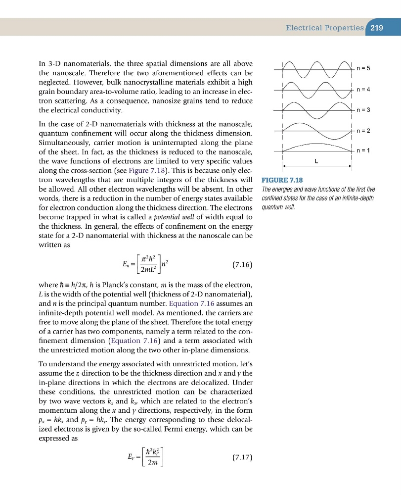
along the cross-section (see Figure 7.18). This is because only electron wavelengths that are multiple integers of the thickness will
be allowed. All other electron wavelengths will be absent. In other
words, there is a reduction in the number of energy states available
for electron conduction along the thickness direction. The electrons
become trapped in what is called a potential well of width equal to
the thickness. In general, the effects of confinement on the energy
state for a 2-D nanomaterial with thickness at the nanoscale can be
written as
E
mL
n
n =
π
2 2
2
2
2
(7.16)
where h – ≡ h/2π, h is Planck’s constant, m is the mass of the electron,
L is the width of the potential well (thickness of 2-D nanomaterial),
and n is the principal quantum number. Equation 7.16 assumes an
infinite-depth potential well model. As mentioned, the carriers are
free to move along the plane of the sheet. Therefore the total energy
of a carrier has two components, namely a term related to the confinement dimension (Equation 7.16) and a term associated with
the unrestricted motion along the two other in-plane dimensions.
To understand the energy associated with unrestricted motion, let’s
assume the z-direction to be the thickness direction and x and y the
in-plane directions in which the electrons are delocalized. Under
these conditions, the unrestricted motion can be characterized
by two wave vectors k x and k x , which are related to the electron’s
momentum along the x and y directions, respectively, in the form
p x = h – k x and p y = h – k y . The energy corresponding to these delocalized electrons is given by the so-called Fermi energy, which can be
expressed as
E
k
m
F
F
=
2 2
2
(7.17)
Figure 7.18
The energies and wave functions of the first five
confined states for the case of an infinite-depth
quantum well.
n = 5
n = 1
n = 2
n = 3
n = 4
L
Electrical Properties
In 3-D nanomaterials, the three spatial dimensions are all above
the nanoscale. Therefore the two aforementioned effects can be
neglected. However, bulk nanocrystalline materials exhibit a high
grain boundary area-to-volume ratio, leading to an increase in electron scattering. As a consequence, nanosize grains tend to reduce
the electrical conductivity.
In the case of 2-D nanomaterials with thickness at the nanoscale,
quantum confinement will occur along the thickness dimension.
Simultaneously, carrier motion is uninterrupted along the plane
of the sheet. In fact, as the thickness is reduced to the nanoscale,
the wave functions of electrons are limited to very specific values
along the cross-section (see Figure 7.18). This is because only electron wavelengths that are multiple integers of the thickness will
be allowed. All other electron wavelengths will be absent. In other
words, there is a reduction in the number of energy states available
for electron conduction along the thickness direction. The electrons
become trapped in what is called a potential well of width equal to
the thickness. In general, the effects of confinement on the energy
state for a 2-D nanomaterial with thickness at the nanoscale can be
written as
E
mL
n
n =
π
2 2
2
2
2
(7.16)
where h – ≡ h/2π, h is Planck’s constant, m is the mass of the electron,
L is the width of the potential well (thickness of 2-D nanomaterial),
and n is the principal quantum number. Equation 7.16 assumes an
infinite-depth potential well model. As mentioned, the carriers are
free to move along the plane of the sheet. Therefore the total energy
of a carrier has two components, namely a term related to the confinement dimension (Equation 7.16) and a term associated with
the unrestricted motion along the two other in-plane dimensions.
To understand the energy associated with unrestricted motion, let’s
assume the z-direction to be the thickness direction and x and y the
in-plane directions in which the electrons are delocalized. Under
these conditions, the unrestricted motion can be characterized
by two wave vectors k x and k x , which are related to the electron’s
momentum along the x and y directions, respectively, in the form
p x = h – k x and p y = h – k y . The energy corresponding to these delocalized electrons is given by the so-called Fermi energy, which can be
expressed as
E
k
m
F
F
=
2 2
2
(7.17)
Figure 7.18
The energies and wave functions of the first five
confined states for the case of an infinite-depth
quantum well.
n = 5
n = 1
n = 2
n = 3
n = 4
L
Electrical Properties