

C hapter 6 nanomaterials: Classes and fundamentals
196
and 2-D, the effects of confinement on the energy state can be
written respectively as
(0-D)
E
mL
n n n
n
x
y
z
=
+ +
(
)
π
2 2
2
2
2
2
2
(6.31a)
(1-D)
E
mL
n n
n
x
y
=
+
(
)
π
2 2
2
2
2
2
(6.31b)
(2-D)
E
mL
n
n
x
=
( )
π
2 2
2
2
2
(6.31c)
where h ¯ ≡ h/2π, h is Planck’s constant, m is the mass of the electron, L is the width (confinement) of the infinitely deep potential
well, and n x , n y , and n z are the principal quantum numbers in the
three dimensions x, y, and z. As shown in Equations 6.31a–c, the
smaller the dimensions of the nanostructure (smaller L), the wider
is the separation between the energy levels, leading to a spectrum of
discreet energies. In this fashion, the band gap of a material can be
shifted toward higher energies by spatially confining the electronic
carriers.
Another important feature of an energy state E n is the number
of conduction electrons, N (E n ), that exist in a particular state.
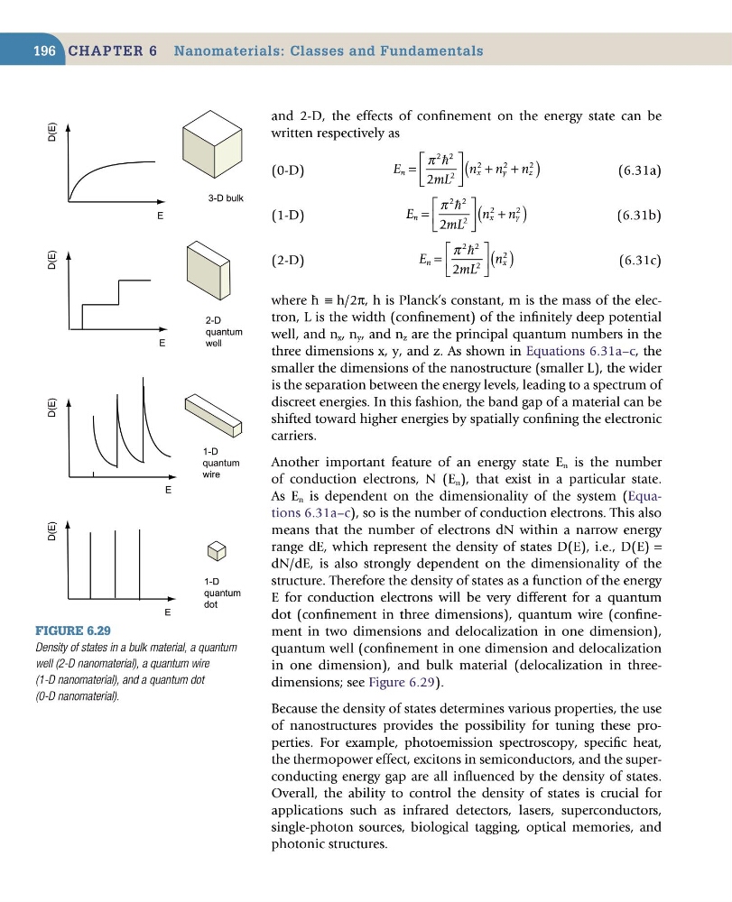
As E n is dependent on the dimensionality of the system (Equations 6.31a–c), so is the number of conduction electrons. This also
means that the number of electrons dN within a narrow energy
range dE, which represent the density of states D(E), i.e., D(E) =
dN/dE, is also strongly dependent on the dimensionality of the
structure. Therefore the density of states as a function of the energy
E for conduction electrons will be very different for a quantum
dot (confinement in three dimensions), quantum wire (confinement in two dimensions and delocalization in one dimension),
quantum well (confinement in one dimension and delocalization
in one dimension), and bulk material (delocalization in threedimensions; see Figure 6.29).
Because the density of states determines various properties, the use
of nanostructures provides the possibility for tuning these properties. For example, photoemission spectroscopy, specific heat,
the thermopower effect, excitons in semiconductors, and the superconducting energy gap are all influenced by the density of states.
Overall, the ability to control the density of states is crucial for
applications such as infrared detectors, lasers, superconductors,
single-photon sources, biological tagging, optical memories, and
photonic structures.
Figure 6.29
Density of states in a bulk material, a quantum
well (2-D nanomaterial), a quantum wire
(1-D nanomaterial), and a quantum dot
(0-D nanomaterial).
E
E
E
E
D(E)
D(E)
D(E)
D(E)
3-D bulk
2-D
quantum
well
1-D
quantum
wire
1-D
quantum
dot
196
and 2-D, the effects of confinement on the energy state can be
written respectively as
(0-D)
E
mL
n n n
n
x
y
z
=
+ +
(
)
π
2 2
2
2
2
2
2
(6.31a)
(1-D)
E
mL
n n
n
x
y
=
+
(
)
π
2 2
2
2
2
2
(6.31b)
(2-D)
E
mL
n
n
x
=
( )
π
2 2
2
2
2
(6.31c)
where h ¯ ≡ h/2π, h is Planck’s constant, m is the mass of the electron, L is the width (confinement) of the infinitely deep potential
well, and n x , n y , and n z are the principal quantum numbers in the
three dimensions x, y, and z. As shown in Equations 6.31a–c, the
smaller the dimensions of the nanostructure (smaller L), the wider
is the separation between the energy levels, leading to a spectrum of
discreet energies. In this fashion, the band gap of a material can be
shifted toward higher energies by spatially confining the electronic
carriers.
Another important feature of an energy state E n is the number
of conduction electrons, N (E n ), that exist in a particular state.
As E n is dependent on the dimensionality of the system (Equations 6.31a–c), so is the number of conduction electrons. This also
means that the number of electrons dN within a narrow energy
range dE, which represent the density of states D(E), i.e., D(E) =
dN/dE, is also strongly dependent on the dimensionality of the
structure. Therefore the density of states as a function of the energy
E for conduction electrons will be very different for a quantum
dot (confinement in three dimensions), quantum wire (confinement in two dimensions and delocalization in one dimension),
quantum well (confinement in one dimension and delocalization
in one dimension), and bulk material (delocalization in threedimensions; see Figure 6.29).
Because the density of states determines various properties, the use
of nanostructures provides the possibility for tuning these properties. For example, photoemission spectroscopy, specific heat,
the thermopower effect, excitons in semiconductors, and the superconducting energy gap are all influenced by the density of states.
Overall, the ability to control the density of states is crucial for
applications such as infrared detectors, lasers, superconductors,
single-photon sources, biological tagging, optical memories, and
photonic structures.
Figure 6.29
Density of states in a bulk material, a quantum
well (2-D nanomaterial), a quantum wire
(1-D nanomaterial), and a quantum dot
(0-D nanomaterial).
E
E
E
E
D(E)
D(E)
D(E)
D(E)
3-D bulk
2-D
quantum
well
1-D
quantum
wire
1-D
quantum
dot