

106
6 Material Modification by High-Power Load …
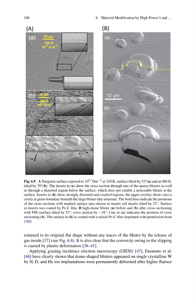
Fig. 6.9 A Tungsten surface exposed to 10 27 Dm −2 at 320 K, surface tilted by 52°(a) and at 480 K,
tilted by 70°(b). The inserts in (a) show the cross section through one of the sparse blisters as well
as through a distorted region below the surface, which does not exhibit a noticeable blister at the
surface. Inserts in (b) show strongly distorted and cracked regions, the upper overlay shows also a
cavity at grain boundary beneath the large blister-like structure. The bold lines indicate the positions
of the cross sections with marked surface area shown in inserts (all inserts tilted by 52°. Surface
in inserts was coated by Pt–C film. B high-dome blister (a) before and (b) after cross sectioning
with FIB (surface tilted by 52°; cross section by −38°. Line in (a) indicates the position of cross
sectioning (b). The surface in (b) is coated with a mixed Pt–C film (reprinted with permission from
[38])
returned to its original flat shape without any traces of the blister by the release of
gas inside [37] (see Fig. 6.8). It is also clear that the convexity owing to the slipping
is caused by plastic deformation [38–41].
Applying grazing incidence electron microscopy (GIEM) [47], Enomoto et al.
[46] have clearly shown that dome-shaped blisters appeared on single crystalline W
by H, D, and He ion implantations were permanently deformed after higher fluence
6 Material Modification by High-Power Load …
Fig. 6.9 A Tungsten surface exposed to 10 27 Dm −2 at 320 K, surface tilted by 52°(a) and at 480 K,
tilted by 70°(b). The inserts in (a) show the cross section through one of the sparse blisters as well
as through a distorted region below the surface, which does not exhibit a noticeable blister at the
surface. Inserts in (b) show strongly distorted and cracked regions, the upper overlay shows also a
cavity at grain boundary beneath the large blister-like structure. The bold lines indicate the positions
of the cross sections with marked surface area shown in inserts (all inserts tilted by 52°. Surface
in inserts was coated by Pt–C film. B high-dome blister (a) before and (b) after cross sectioning
with FIB (surface tilted by 52°; cross section by −38°. Line in (a) indicates the position of cross
sectioning (b). The surface in (b) is coated with a mixed Pt–C film (reprinted with permission from
[38])
returned to its original flat shape without any traces of the blister by the release of
gas inside [37] (see Fig. 6.8). It is also clear that the convexity owing to the slipping
is caused by plastic deformation [38–41].
Applying grazing incidence electron microscopy (GIEM) [47], Enomoto et al.
[46] have clearly shown that dome-shaped blisters appeared on single crystalline W
by H, D, and He ion implantations were permanently deformed after higher fluence