

354
NANOMACHINES AND NANODEVICES
t ”
‘ OUT
A 0
1
I B O 1
0
-
1
1
0
1
AND gate address levels
-1 ’
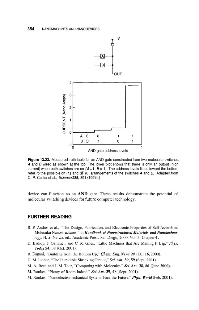
Figure 13.23. Measured truth table for an AND gate constructed from two molecular switches
A and B wired as shown at the top. The lower plot shows that there is only an output (high
current) when both switches are on ( A = 1, B= 1). The address levels listed toward the bottom
refer to the possible on (1) and off (0) arrangements of the switches A and B. [Adapted from
C. P. Collier et al., Science 285, 391 (1999).]
device can finction as an AND gate. These results demonstrate the potential of
molecular switching devices for fiture computer technology.
FURTHER READING
R. F! Andres et al., “The Design, Fabrication, and Electronic Properties of Self Assembled
Molecular Nanostructures,” in Handbook of Nanostructured Materials and NanotechnoLogy, H. S . Nalwa, ed., Academic Press, San Diego, 2000, Vol. 3, Chapter 4.
D. Bishop, F! Gammel, and C. R. Giles, “Little Machines that Are Making It Big,” Phys.
Today 54, 38 (Oct. 2001).
R. Dagani, “Building from the Bottom Up,” Chem. Eng. News 28 (Oct 16, 2000).
C. M. Lieber, “The Incredible Shrinking Circuit,” Scz. Am. 39, 59 (Sept. 2001).
M. A. Reed and J. M. Tour, “Computing with Molecules,” Sci. Am. 38, 86 (June 2000).
M. Roukes, “Plenty of Room Indeed,” Sci. Am. 39,48 (Sept. 2001).
M. Roukes, “Nanoelectromechanical Systems Face the Future,” Phys. World (Feb. 200 1).
NANOMACHINES AND NANODEVICES
t ”
‘ OUT
A 0
1
I B O 1
0
-
1
1
0
1
AND gate address levels
-1 ’
Figure 13.23. Measured truth table for an AND gate constructed from two molecular switches
A and B wired as shown at the top. The lower plot shows that there is only an output (high
current) when both switches are on ( A = 1, B= 1). The address levels listed toward the bottom
refer to the possible on (1) and off (0) arrangements of the switches A and B. [Adapted from
C. P. Collier et al., Science 285, 391 (1999).]
device can finction as an AND gate. These results demonstrate the potential of
molecular switching devices for fiture computer technology.
FURTHER READING
R. F! Andres et al., “The Design, Fabrication, and Electronic Properties of Self Assembled
Molecular Nanostructures,” in Handbook of Nanostructured Materials and NanotechnoLogy, H. S . Nalwa, ed., Academic Press, San Diego, 2000, Vol. 3, Chapter 4.
D. Bishop, F! Gammel, and C. R. Giles, “Little Machines that Are Making It Big,” Phys.
Today 54, 38 (Oct. 2001).
R. Dagani, “Building from the Bottom Up,” Chem. Eng. News 28 (Oct 16, 2000).
C. M. Lieber, “The Incredible Shrinking Circuit,” Scz. Am. 39, 59 (Sept. 2001).
M. A. Reed and J. M. Tour, “Computing with Molecules,” Sci. Am. 38, 86 (June 2000).
M. Roukes, “Plenty of Room Indeed,” Sci. Am. 39,48 (Sept. 2001).
M. Roukes, “Nanoelectromechanical Systems Face the Future,” Phys. World (Feb. 200 1).