

338
NANOMACHINES AND NANODEVICES
tip
tip trajectory
\
I
surface
V - - - bond
CCCCCOCO
(b)
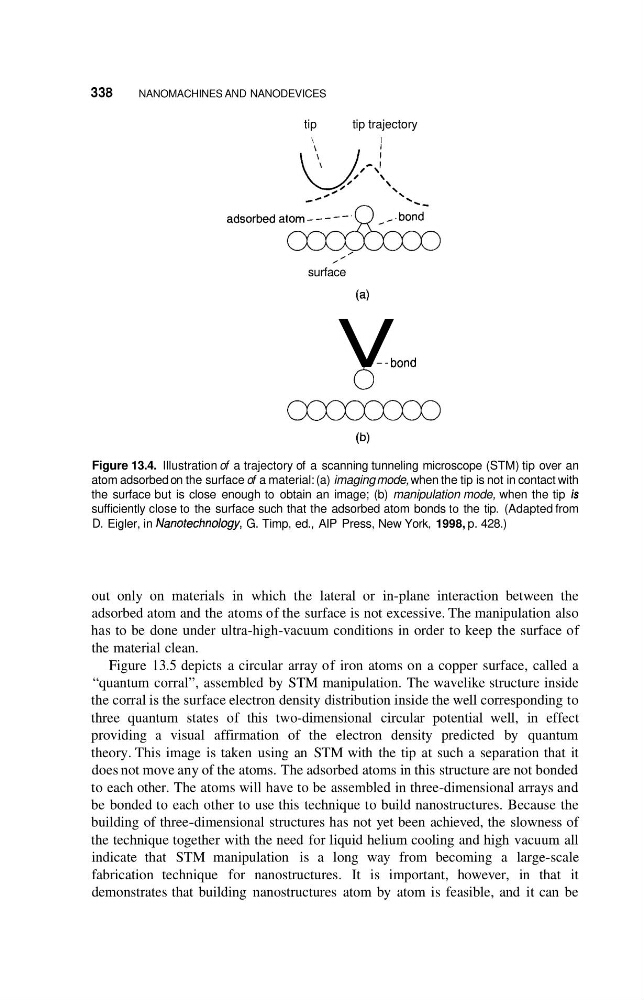
Figure 13.4. Illustration of a trajectory of a scanning tunneling microscope (STM) tip over an
atom adsorbed on the surface of a material: (a) imaging mode, when the tip is not in contact with
the surface but is close enough to obtain an image; (b) manipulation mode, when the tip is
sufficiently close to the surface such that the adsorbed atom bonds to the tip. (Adapted from
D. Eigler, in Nanotechno/ogy, G. Timp, ed., AIP Press, New York, 1998, p. 428.)
out only on materials in which the lateral or in-plane interaction between the
adsorbed atom and the atoms of the surface is not excessive. The manipulation also
has to be done under ultra-high-vacuum conditions in order to keep the surface of
the material clean.
Figure 13.5 depicts a circular array of iron atoms on a copper surface, called a
“quantum corral”, assembled by STM manipulation. The wavelike structure inside
the corral is the surface electron density distribution inside the well corresponding to
three quantum states of this two-dimensional circular potential well, in effect
providing a visual affirmation of the electron density predicted by quantum
theory. This image is taken using an STM with the tip at such a separation that it
does not move any of the atoms. The adsorbed atoms in this structure are not bonded
to each other. The atoms will have to be assembled in three-dimensional arrays and
be bonded to each other to use this technique to build nanostructures. Because the
building of three-dimensional structures has not yet been achieved, the slowness of
the technique together with the need for liquid helium cooling and high vacuum all
indicate that STM manipulation is a long way from becoming a large-scale
fabrication technique for nanostructures. It is important, however, in that it
demonstrates that building nanostructures atom by atom is feasible, and it can be
NANOMACHINES AND NANODEVICES
tip
tip trajectory
\
I
surface
V - - - bond
CCCCCOCO
(b)
Figure 13.4. Illustration of a trajectory of a scanning tunneling microscope (STM) tip over an
atom adsorbed on the surface of a material: (a) imaging mode, when the tip is not in contact with
the surface but is close enough to obtain an image; (b) manipulation mode, when the tip is
sufficiently close to the surface such that the adsorbed atom bonds to the tip. (Adapted from
D. Eigler, in Nanotechno/ogy, G. Timp, ed., AIP Press, New York, 1998, p. 428.)
out only on materials in which the lateral or in-plane interaction between the
adsorbed atom and the atoms of the surface is not excessive. The manipulation also
has to be done under ultra-high-vacuum conditions in order to keep the surface of
the material clean.
Figure 13.5 depicts a circular array of iron atoms on a copper surface, called a
“quantum corral”, assembled by STM manipulation. The wavelike structure inside
the corral is the surface electron density distribution inside the well corresponding to
three quantum states of this two-dimensional circular potential well, in effect
providing a visual affirmation of the electron density predicted by quantum
theory. This image is taken using an STM with the tip at such a separation that it
does not move any of the atoms. The adsorbed atoms in this structure are not bonded
to each other. The atoms will have to be assembled in three-dimensional arrays and
be bonded to each other to use this technique to build nanostructures. Because the
building of three-dimensional structures has not yet been achieved, the slowness of
the technique together with the need for liquid helium cooling and high vacuum all
indicate that STM manipulation is a long way from becoming a large-scale
fabrication technique for nanostructures. It is important, however, in that it
demonstrates that building nanostructures atom by atom is feasible, and it can be