

246
QUANTUM WELLS, WIRES, AND DOTS
removes electrons for use in the external circuit. The applied voltage V,, causes
direct current I to flow, with electrons tunneling into and out of the quantum dot. In
accordance with Ohm’s law V = IR, the current flow I through the circuit of Fig. 9.16
equals the applied source-drain voltage V,, divided by the resistance R, and the main
contribution to the value of R arises from the process of electron tunneling from
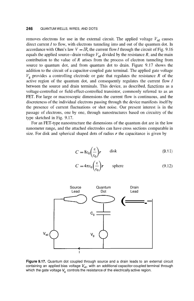
source to quantum dot, and from quantum dot to drain. Figure 9.17 shows the
addition to the circuit of a capacitor-coupled gate terminal. The applied gate voltage
Vg provides a controlling electrode or gate that regulates the resistance R of the
active region of the quantum dot, and consequently regulates the current flow I
between the source and drain terminals. This device, as described, hnctions as a
voltage-controlled or field-effect-controlled transistor, commonly referred to as an
FET. For large or macroscopic dimensions the current flow is continuous, and the
discreteness of the individual electrons passing through the device manifests itself by
the presence of current fluctuations or shot noise. Our present interest is in the
passage of electrons, one by one, through nanostructures based on circuitry of the
type sketched in Fig. 9.17.
For an FET-type nanostructure the dimensions of the quantum dot are in the low
nanometer range, and the attached electrodes can have cross sections comparable in
size. For disk and spherical shaped dots of radius r the capacitance is given by
C = 8~~ (t) r disk
C = 4m0 (
:
) r sphere
Source
Lead
vsd
Quantum
Dot
0
Drain
Lead
(==.(9.1 I )
(9.12)
Figure 9.17. Quantum dot coupled through source and a drain leads to an external circuit
containing an applied bias voltage V,,, with an additional capacitor-coupled terminal through
which the gate voltage Vg controls the resistance of the electrically active region.
QUANTUM WELLS, WIRES, AND DOTS
removes electrons for use in the external circuit. The applied voltage V,, causes
direct current I to flow, with electrons tunneling into and out of the quantum dot. In
accordance with Ohm’s law V = IR, the current flow I through the circuit of Fig. 9.16
equals the applied source-drain voltage V,, divided by the resistance R, and the main
contribution to the value of R arises from the process of electron tunneling from
source to quantum dot, and from quantum dot to drain. Figure 9.17 shows the
addition to the circuit of a capacitor-coupled gate terminal. The applied gate voltage
Vg provides a controlling electrode or gate that regulates the resistance R of the
active region of the quantum dot, and consequently regulates the current flow I
between the source and drain terminals. This device, as described, hnctions as a
voltage-controlled or field-effect-controlled transistor, commonly referred to as an
FET. For large or macroscopic dimensions the current flow is continuous, and the
discreteness of the individual electrons passing through the device manifests itself by
the presence of current fluctuations or shot noise. Our present interest is in the
passage of electrons, one by one, through nanostructures based on circuitry of the
type sketched in Fig. 9.17.
For an FET-type nanostructure the dimensions of the quantum dot are in the low
nanometer range, and the attached electrodes can have cross sections comparable in
size. For disk and spherical shaped dots of radius r the capacitance is given by
C = 8~~ (t) r disk
C = 4m0 (
:
) r sphere
Source
Lead
vsd
Quantum
Dot
0
Drain
Lead
(==.(9.1 I )
(9.12)
Figure 9.17. Quantum dot coupled through source and a drain leads to an external circuit
containing an applied bias voltage V,,, with an additional capacitor-coupled terminal through
which the gate voltage Vg controls the resistance of the electrically active region.