

152
BULK NANOSTRUCTURED MATERIALS
Backside
Electrical -+
Connection
Pt Electrode
Si Wafer
\ I Etching Solution, HF
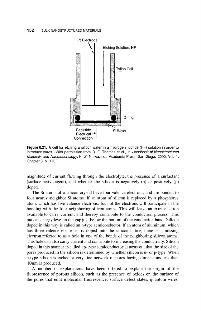
Figure 6.21. A cell for etching a silicon wafer in a hydrogen fluoride (HF) solution in order to
introduce pores. (With permission from D. F. Thomas et al., in Handbook of Nanostructured
Materials and Nanotechnology, H. S. Nalwa, ed., Academic Press, San Diego, 2000, Vol. 4,
Chapter 3, p. 173.)
magnitude of current flowing through the electrolyte, the presence of a surfactant
(surface-active agent), and whether the silicon is negatively (n) or positively (p)
doped.
The Si atoms of a silicon crystal have four valence electrons, and are bonded to
four nearest-neighbor Si atoms. If an atom of silicon is replaced by a phosphorus
atom, which has five valence electrons, four of the electrons will participate in the
bonding with the four neighboring silicon atoms. This will leave an extra electron
available to carry current, and thereby contribute to the conduction process. This
puts an energy level in the gap just below the bottom of the conduction band. Silicon
doped in this way is called an n-type semiconductor. If an atom of aluminum, which
has three valence electrons, is doped into the silicon lattice, there is a missing
electron referred to as a hole in one of the bonds of the neighboring silicon atoms.
This hole can also carry current and contribute to increasing the conductivity. Silicon
doped in this manner is called ap-type semiconductor: It turns out that the size of the
pores produced in the silicon is determined by whether silicon is n- or p-type. When
p-type silicon is etched, a very fine network of pores having dimensions less than
10 nm is produced.
A number of explanations have been offered to explain the origin of the
fluorescence of porous silicon, such as the presence of oxides on the surface of
the pores that emit molecular fluorescence, surface defect states, quantum wires,
BULK NANOSTRUCTURED MATERIALS
Backside
Electrical -+
Connection
Pt Electrode
Si Wafer
\ I Etching Solution, HF
Figure 6.21. A cell for etching a silicon wafer in a hydrogen fluoride (HF) solution in order to
introduce pores. (With permission from D. F. Thomas et al., in Handbook of Nanostructured
Materials and Nanotechnology, H. S. Nalwa, ed., Academic Press, San Diego, 2000, Vol. 4,
Chapter 3, p. 173.)
magnitude of current flowing through the electrolyte, the presence of a surfactant
(surface-active agent), and whether the silicon is negatively (n) or positively (p)
doped.
The Si atoms of a silicon crystal have four valence electrons, and are bonded to
four nearest-neighbor Si atoms. If an atom of silicon is replaced by a phosphorus
atom, which has five valence electrons, four of the electrons will participate in the
bonding with the four neighboring silicon atoms. This will leave an extra electron
available to carry current, and thereby contribute to the conduction process. This
puts an energy level in the gap just below the bottom of the conduction band. Silicon
doped in this way is called an n-type semiconductor. If an atom of aluminum, which
has three valence electrons, is doped into the silicon lattice, there is a missing
electron referred to as a hole in one of the bonds of the neighboring silicon atoms.
This hole can also carry current and contribute to increasing the conductivity. Silicon
doped in this manner is called ap-type semiconductor: It turns out that the size of the
pores produced in the silicon is determined by whether silicon is n- or p-type. When
p-type silicon is etched, a very fine network of pores having dimensions less than
10 nm is produced.
A number of explanations have been offered to explain the origin of the
fluorescence of porous silicon, such as the presence of oxides on the surface of
the pores that emit molecular fluorescence, surface defect states, quantum wires,