

126
CARBON NANOSTRUCTURES
5.5.2. Computers
The feasibility of designing field-effect transistors (FETs), the switching components
of computers, based on semiconducting carbon nanotubes connecting two gold
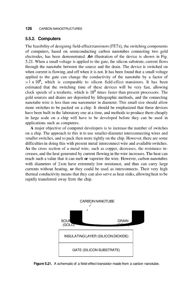
electrodes, has been demonstrated. An illustration of the device is shown in Fig.
5.21. When a small voltage is applied to the gate, the silicon substrate, current flows
through the nanotube between the source and the drain. The device is switched on
when current is flowing, and off when it is not. It has been found that a small voltage
applied to the gate can change the conductivity of the nanotube by a factor of
> 1 x lo6, which is comparable to silicon field-effect transistors. It has been
estimated that the switching time of these devices will be very fast, allowing
clock speeds of a terahertz, which is lo4 times faster than present processors. The
gold sources and drains are deposited by lithographic methods, and the connecting
nanotube wire is less than one nanometer in diameter. This small size should allow
more switches to be packed on a chip. It should be emphasized that these devices
have been built in the laboratory one at a time, and methods to produce them cheaply
in large scale on a chip will have to be developed before they can be used in
applications such as computers.
A major objective of computer developers is to increase the number of switches
on a chip. The approach to this is to use smaller-diameter interconnecting wires and
smaller switches, and to pack then more tightly on the chip. However, there are some
difficulties in doing this with present metal interconnect wire and available switches.
As the cross section of a metal wire, such as copper, decreases, the resistance increases, and the heat generated by current flowing in the wire increases. The heat can
reach such a value that it can melt or vaporize the wire. However, carbon nanotubes
with diameters of 2 n m have extremely low resistance, and thus can carry large
currents without heating, so they could be used as interconnects. Their very high
thermal conductivity means that they can also serve as heat sinks, allowing heat to be
rapidly transferred away from the chip.
CARBON NANOTUBE
/*
/
SOURCE
DRAIN
U (GOLD)
(GOLD)
INSULATING LAYER (SILICON DIOXIDE)
GATE (SILICON SUBSTRATE)
Figure 5.21. A schematic of a field-effect transistor made from a carbon nanotube.
CARBON NANOSTRUCTURES
5.5.2. Computers
The feasibility of designing field-effect transistors (FETs), the switching components
of computers, based on semiconducting carbon nanotubes connecting two gold
electrodes, has been demonstrated. An illustration of the device is shown in Fig.
5.21. When a small voltage is applied to the gate, the silicon substrate, current flows
through the nanotube between the source and the drain. The device is switched on
when current is flowing, and off when it is not. It has been found that a small voltage
applied to the gate can change the conductivity of the nanotube by a factor of
> 1 x lo6, which is comparable to silicon field-effect transistors. It has been
estimated that the switching time of these devices will be very fast, allowing
clock speeds of a terahertz, which is lo4 times faster than present processors. The
gold sources and drains are deposited by lithographic methods, and the connecting
nanotube wire is less than one nanometer in diameter. This small size should allow
more switches to be packed on a chip. It should be emphasized that these devices
have been built in the laboratory one at a time, and methods to produce them cheaply
in large scale on a chip will have to be developed before they can be used in
applications such as computers.
A major objective of computer developers is to increase the number of switches
on a chip. The approach to this is to use smaller-diameter interconnecting wires and
smaller switches, and to pack then more tightly on the chip. However, there are some
difficulties in doing this with present metal interconnect wire and available switches.
As the cross section of a metal wire, such as copper, decreases, the resistance increases, and the heat generated by current flowing in the wire increases. The heat can
reach such a value that it can melt or vaporize the wire. However, carbon nanotubes
with diameters of 2 n m have extremely low resistance, and thus can carry large
currents without heating, so they could be used as interconnects. Their very high
thermal conductivity means that they can also serve as heat sinks, allowing heat to be
rapidly transferred away from the chip.
CARBON NANOTUBE
/*
/
SOURCE
DRAIN
U (GOLD)
(GOLD)
INSULATING LAYER (SILICON DIOXIDE)
GATE (SILICON SUBSTRATE)
Figure 5.21. A schematic of a field-effect transistor made from a carbon nanotube.