

E1C11 09/14/2010
13:14:2 Page 475
Semiconductor Strain Gauges
When subjected to a load, a semiconductor material exhibits a change in resistance, and therefore
can be used for the measurement of strain. Silicon crystals are the basic material for semiconductor
strain gauges; the crystals are sliced into very thin sections to form strain gauges. Mounting such
gauges in a transducer, such as a pressure transducer, or on a test specimen requires backing and
adhesive techniques similar to those used for metallic gauges. Because of the large piezoresistance
coefficient, the semiconductor gauge exhibits a very large gauge factor, as large as 200 for some
gauges. These gauges also exhibit higher resistance, longer fatigue life, and lower hysteresis under
some conditions than metallic gauges. However, the output of the semiconductor strain gauge is
nonlinear with strain, and the strain sensitivity or gauge factor may be markedly dependent on
temperature.
Semiconductor materials for strain gauge applications have resistivities ranging from 10
À6 to
10
À2
V-m. Semiconductor strain gauges may have a relatively high or low density of charge carriers
(3, 7). Semiconductor strain gauges made of materials having a relatively high density of charge
carriers ($10
20 carriers/cm
3 ) exhibit little variation of their gauge factor with strain or temperature.
On the other hand, for the case where the crystal contains a low number of charge carriers (<10
17
carriers/cm
3 ), the gauge factor may be approximated as
GF ¼
T 0
T
GF 0 þ C 1
T 0
T
2
e
ð11:13Þ
where GF 0 is the gauge factor at the reference temperature T 0 , under conditions of zero strain (8),
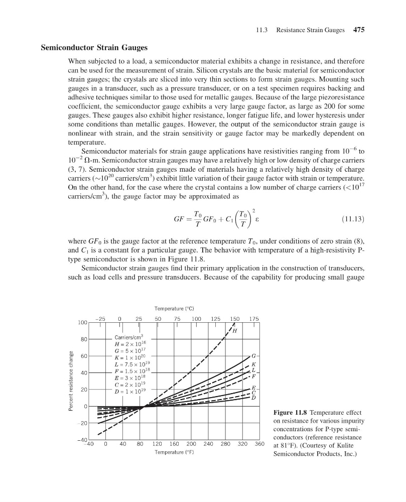
and C 1 is a constant for a particular gauge. The behavior with temperature of a high-resistivity Ptype semiconductor is shown in Figure 11.8.
Semiconductor strain gauges find their primary application in the construction of transducers,
such as load cells and pressure transducers. Because of the capability for producing small gauge
–40
0
–25
0
25
50
75
100
125
150
175
40
80
120 160 200 240 280 320 360
H
Temperature (°F)
Temperature (°C)
Percent resistance change
–40
–20
0
20
40
60
80
100
Carriers/cm
3
H = 2 × 10
16
G = 5 × 10
17
K = 1 × 10
20
L = 7.5 × 10
19
F = 1.5 × 10
18
E = 3 × 10
18
C = 2 × 10
19
D = 1 × 10
19
G
K
L
F
E
D
C
Figure 11.8 Temperature effect
on resistance for various impurity
concentrations for P-type semiconductors (reference resistance
at 81
F). (Courtesy of Kulite
Semiconductor Products, Inc.)
11.3 Resistance Strain Gauges 475
13:14:2 Page 475
Semiconductor Strain Gauges
When subjected to a load, a semiconductor material exhibits a change in resistance, and therefore
can be used for the measurement of strain. Silicon crystals are the basic material for semiconductor
strain gauges; the crystals are sliced into very thin sections to form strain gauges. Mounting such
gauges in a transducer, such as a pressure transducer, or on a test specimen requires backing and
adhesive techniques similar to those used for metallic gauges. Because of the large piezoresistance
coefficient, the semiconductor gauge exhibits a very large gauge factor, as large as 200 for some
gauges. These gauges also exhibit higher resistance, longer fatigue life, and lower hysteresis under
some conditions than metallic gauges. However, the output of the semiconductor strain gauge is
nonlinear with strain, and the strain sensitivity or gauge factor may be markedly dependent on
temperature.
Semiconductor materials for strain gauge applications have resistivities ranging from 10
À6 to
10
À2
V-m. Semiconductor strain gauges may have a relatively high or low density of charge carriers
(3, 7). Semiconductor strain gauges made of materials having a relatively high density of charge
carriers ($10
20 carriers/cm
3 ) exhibit little variation of their gauge factor with strain or temperature.
On the other hand, for the case where the crystal contains a low number of charge carriers (<10
17
carriers/cm
3 ), the gauge factor may be approximated as
GF ¼
T 0
T
GF 0 þ C 1
T 0
T
2
e
ð11:13Þ
where GF 0 is the gauge factor at the reference temperature T 0 , under conditions of zero strain (8),
and C 1 is a constant for a particular gauge. The behavior with temperature of a high-resistivity Ptype semiconductor is shown in Figure 11.8.
Semiconductor strain gauges find their primary application in the construction of transducers,
such as load cells and pressure transducers. Because of the capability for producing small gauge
–40
0
–25
0
25
50
75
100
125
150
175
40
80
120 160 200 240 280 320 360
H
Temperature (°F)
Temperature (°C)
Percent resistance change
–40
–20
0
20
40
60
80
100
Carriers/cm
3
H = 2 × 10
16
G = 5 × 10
17
K = 1 × 10
20
L = 7.5 × 10
19
F = 1.5 × 10
18
E = 3 × 10
18
C = 2 × 10
19
D = 1 × 10
19
G
K
L
F
E
D
C
Figure 11.8 Temperature effect
on resistance for various impurity
concentrations for P-type semiconductors (reference resistance
at 81
F). (Courtesy of Kulite
Semiconductor Products, Inc.)
11.3 Resistance Strain Gauges 475