

E1C06 09/14/2010
11:55:6 Page 232
The differential amplifier circuit is effective as a voltage comparator for many instrument
applications (see Section 6.7).
A voltage follower circuit is commonly used to isolate an impedance load from other stages of a
measurement system, such as might be needed with a high-output impedance transducer. A
schematic diagram of a voltage follower circuit is shown in Figure 6.20d. Note that the feedback
4.5 kΩ
25 Ω
7.5 kΩ
39 kΩ
50 Ω
50 Ω
50 kΩ
5 kΩ
50 kΩ
1 kΩ
1kΩ
30 pF
E i 2
Noninverting
input (+)
E o
output
E i 1
Inverting
input (–)
Bias
(offset
null)
(3)
(7)
(6)
(4)
(2)
(1)
(5)
(c) Type 741 circuit diagram
dc +
dc –
E o
Output
E i1
E i2
(a) Circuit representation
(b) 8–pin mini-dip Type 741
Inverting input
Noninverting
input (+)
dc
+ dc
–
Offset
null
(bias)
Offset
null
(bias)
Inverting
input
Noninverting
input
dc
–
dc
+
NC
Output
1
2
3
4
8
7
6
5
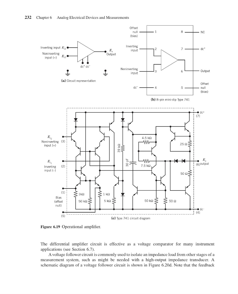
Figure 6.19 Operational amplifier.
232 Chapter 6 Analog Electrical Devices and Measurements
11:55:6 Page 232
The differential amplifier circuit is effective as a voltage comparator for many instrument
applications (see Section 6.7).
A voltage follower circuit is commonly used to isolate an impedance load from other stages of a
measurement system, such as might be needed with a high-output impedance transducer. A
schematic diagram of a voltage follower circuit is shown in Figure 6.20d. Note that the feedback
4.5 kΩ
25 Ω
7.5 kΩ
39 kΩ
50 Ω
50 Ω
50 kΩ
5 kΩ
50 kΩ
1 kΩ
1kΩ
30 pF
E i 2
Noninverting
input (+)
E o
output
E i 1
Inverting
input (–)
Bias
(offset
null)
(3)
(7)
(6)
(4)
(2)
(1)
(5)
(c) Type 741 circuit diagram
dc +
dc –
E o
Output
E i1
E i2
(a) Circuit representation
(b) 8–pin mini-dip Type 741
Inverting input
Noninverting
input (+)
dc
+ dc
–
Offset
null
(bias)
Offset
null
(bias)
Inverting
input
Noninverting
input
dc
–
dc
+
NC
Output
1
2
3
4
8
7
6
5
Figure 6.19 Operational amplifier.
232 Chapter 6 Analog Electrical Devices and Measurements