

10.6 Spintronics Sensors
251
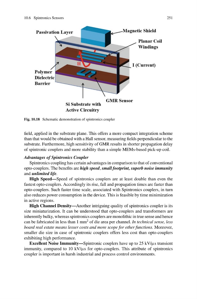
Fig. 10.18 Schematic demonstration of spintronics coupler
field, applied in the substrate plane. This offers a more compact integration scheme
than that would be obtained with a Hall sensor, measuring fields perpendicular to the
substrate. Furthermore, high sensitivity of GMR results in shorter propagation delay
of spintronic couplers and more stability than a simple MEMs-based pick-up coil.
Advantages of Spintronics Coupler
Spintronics coupling has certain advantages in comparison to that of conventional
opto-couplers. The benefits are high speed, small footprint, superb noise immunity
and unlimited life.
High Speed—Speed of spintronics couplers are at least double than even the
fastest opto-couplers. Accordingly its rise, fall and propagation times are faster than
opto-couplers. Such faster time scale, associated with Spintronics couplers, in turn
also reduces power consumption in the device. This is feasible by time minimization
in active regions.
High Channel Density—Another intriguing quality of spintronics coupler is its
size miniaturization. It can be understood that opto-couplers and transformers are
inherently bulky, whereas spintronics couplers are monolithic in true sense and hence
can be fabricated in less than 1 mm
2 of die area per channel. In technical sense, less
board real estate means lesser costs and more scope for other functions. Moreover,
smaller die size in case of spintronic couplers offers less cost than opto-couplers
exhibiting high performance.
Excellent Noise Immunity—Spintronic couplers have up to 25 kV/μs transient
immunity, compared to 10 kV/μs for opto-couplers. This attribute of spintronics
coupler is important in harsh industrial and process control environments.
251
Fig. 10.18 Schematic demonstration of spintronics coupler
field, applied in the substrate plane. This offers a more compact integration scheme
than that would be obtained with a Hall sensor, measuring fields perpendicular to the
substrate. Furthermore, high sensitivity of GMR results in shorter propagation delay
of spintronic couplers and more stability than a simple MEMs-based pick-up coil.
Advantages of Spintronics Coupler
Spintronics coupling has certain advantages in comparison to that of conventional
opto-couplers. The benefits are high speed, small footprint, superb noise immunity
and unlimited life.
High Speed—Speed of spintronics couplers are at least double than even the
fastest opto-couplers. Accordingly its rise, fall and propagation times are faster than
opto-couplers. Such faster time scale, associated with Spintronics couplers, in turn
also reduces power consumption in the device. This is feasible by time minimization
in active regions.
High Channel Density—Another intriguing quality of spintronics coupler is its
size miniaturization. It can be understood that opto-couplers and transformers are
inherently bulky, whereas spintronics couplers are monolithic in true sense and hence
can be fabricated in less than 1 mm
2 of die area per channel. In technical sense, less
board real estate means lesser costs and more scope for other functions. Moreover,
smaller die size in case of spintronic couplers offers less cost than opto-couplers
exhibiting high performance.
Excellent Noise Immunity—Spintronic couplers have up to 25 kV/μs transient
immunity, compared to 10 kV/μs for opto-couplers. This attribute of spintronics
coupler is important in harsh industrial and process control environments.