

9.2 Issues to Be Considered
203
(2) Decrease of spin lifetime: To lessen the conductivity mismatch, the doping
concentration of the semiconductor is increased. This intern would reduce the
spin lifetime due to the aggravated spin relaxation from impurity scattering.
(3) The localized states at the FM/SC interface and the surface roughness could
considerably make matters worse and put at risk the spin injection process.
9.3 Materials, Structures and Spin Injection
There are several methods for achieving formation, injection and detection of spin
in semiconductors (De Cesari et al. 2017).
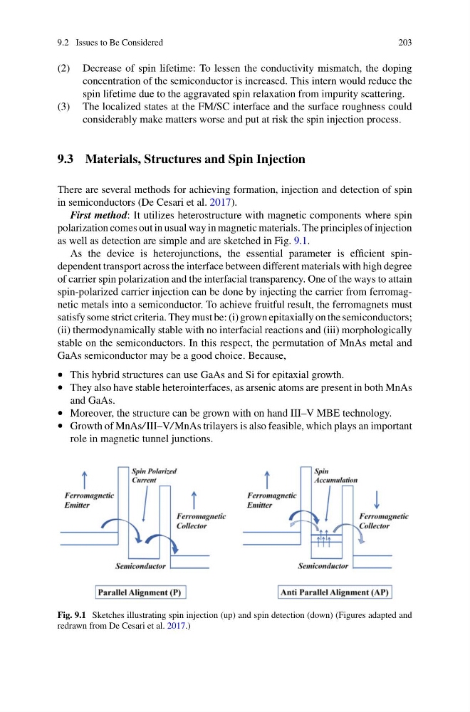
First method: It utilizes heterostructure with magnetic components where spin
polarization comes out in usual way in magnetic materials. The principles of injection
as well as detection are simple and are sketched in Fig. 9.1.
As the device is heterojunctions, the essential parameter is efficient spindependent transport across the interface between different materials with high degree
of carrier spin polarization and the interfacial transparency. One of the ways to attain
spin-polarized carrier injection can be done by injecting the carrier from ferromagnetic metals into a semiconductor. To achieve fruitful result, the ferromagnets must
satisfy some strict criteria. They must be: (i) grown epitaxially on the semiconductors;
(ii) thermodynamically stable with no interfacial reactions and (iii) morphologically
stable on the semiconductors. In this respect, the permutation of MnAs metal and
GaAs semiconductor may be a good choice. Because,
• This hybrid structures can use GaAs and Si for epitaxial growth.
• They also have stable heterointerfaces, as arsenic atoms are present in both MnAs
and GaAs.
• Moreover, the structure can be grown with on hand III–V MBE technology.
• Growth of MnAs/ III–V/ MnAs trilayers is also feasible, which plays an important
role in magnetic tunnel junctions.
Fig. 9.1 Sketches illustrating spin injection (up) and spin detection (down) (Figures adapted and
redrawn from De Cesari et al. 2017.)
203
(2) Decrease of spin lifetime: To lessen the conductivity mismatch, the doping
concentration of the semiconductor is increased. This intern would reduce the
spin lifetime due to the aggravated spin relaxation from impurity scattering.
(3) The localized states at the FM/SC interface and the surface roughness could
considerably make matters worse and put at risk the spin injection process.
9.3 Materials, Structures and Spin Injection
There are several methods for achieving formation, injection and detection of spin
in semiconductors (De Cesari et al. 2017).
First method: It utilizes heterostructure with magnetic components where spin
polarization comes out in usual way in magnetic materials. The principles of injection
as well as detection are simple and are sketched in Fig. 9.1.
As the device is heterojunctions, the essential parameter is efficient spindependent transport across the interface between different materials with high degree
of carrier spin polarization and the interfacial transparency. One of the ways to attain
spin-polarized carrier injection can be done by injecting the carrier from ferromagnetic metals into a semiconductor. To achieve fruitful result, the ferromagnets must
satisfy some strict criteria. They must be: (i) grown epitaxially on the semiconductors;
(ii) thermodynamically stable with no interfacial reactions and (iii) morphologically
stable on the semiconductors. In this respect, the permutation of MnAs metal and
GaAs semiconductor may be a good choice. Because,
• This hybrid structures can use GaAs and Si for epitaxial growth.
• They also have stable heterointerfaces, as arsenic atoms are present in both MnAs
and GaAs.
• Moreover, the structure can be grown with on hand III–V MBE technology.
• Growth of MnAs/ III–V/ MnAs trilayers is also feasible, which plays an important
role in magnetic tunnel junctions.
Fig. 9.1 Sketches illustrating spin injection (up) and spin detection (down) (Figures adapted and
redrawn from De Cesari et al. 2017.)