

4.2 Hardware Verification of the Digital Design
107
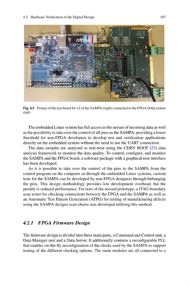
Fig. 4.5 Picture of the test board for v2 of the SAMPA (right) connected to the FPGA DAQ system
(left)
The embedded Linux system has full access to the stream of incoming data as well
as the possibility to take over the control of all pins on the SAMPA, providing a lower
threshold for non-FPGA developers to develop test and verification applications
directly on the embedded system without the need to use the UART connection.
The data samples are analysed in real-time using the CERN ROOT [23] data
analysis framework to monitor the data quality. To control, configure, and monitor
the SAMPA and the FPGA board, a software package with a graphical user interface
has been developed.
As it is possible to take over the control of the pins to the SAMPA from the
control program on the computer or through the embedded Linux systems, custom
tests for the SAMPA can be developed by non-FPGA designers through bitbanging
the pins. This design methodology provides low development overhead, but the
penalty is reduced performance. For tests of the second prototype, a JTAG boundary
scan tester for checking connections between the FPGA and the SAMPA as well as
an Automatic Test Pattern Generation (ATPG) for testing of manufacturing defects
using the SAMPA designs scan chains was developed utilizing this method.
4.2.1 FPGA Firmware Design
The firmware design is divided into three main parts, a Command and Control unit, a
Data Manager unit and a Data Server. It additionally contains a reconfigurable PLL
that enables on-the-fly reconfiguration of the clocks used by the SAMPA to support
testing of the different clocking options. The main modules are all connected to a
107
Fig. 4.5 Picture of the test board for v2 of the SAMPA (right) connected to the FPGA DAQ system
(left)
The embedded Linux system has full access to the stream of incoming data as well
as the possibility to take over the control of all pins on the SAMPA, providing a lower
threshold for non-FPGA developers to develop test and verification applications
directly on the embedded system without the need to use the UART connection.
The data samples are analysed in real-time using the CERN ROOT [23] data
analysis framework to monitor the data quality. To control, configure, and monitor
the SAMPA and the FPGA board, a software package with a graphical user interface
has been developed.
As it is possible to take over the control of the pins to the SAMPA from the
control program on the computer or through the embedded Linux systems, custom
tests for the SAMPA can be developed by non-FPGA designers through bitbanging
the pins. This design methodology provides low development overhead, but the
penalty is reduced performance. For tests of the second prototype, a JTAG boundary
scan tester for checking connections between the FPGA and the SAMPA as well as
an Automatic Test Pattern Generation (ATPG) for testing of manufacturing defects
using the SAMPA designs scan chains was developed utilizing this method.
4.2.1 FPGA Firmware Design
The firmware design is divided into three main parts, a Command and Control unit, a
Data Manager unit and a Data Server. It additionally contains a reconfigurable PLL
that enables on-the-fly reconfiguration of the clocks used by the SAMPA to support
testing of the different clocking options. The main modules are all connected to a