

20
1 Electromagnetics for Zero-Index Metamaterials
(a)
(b)
(c)
(d)
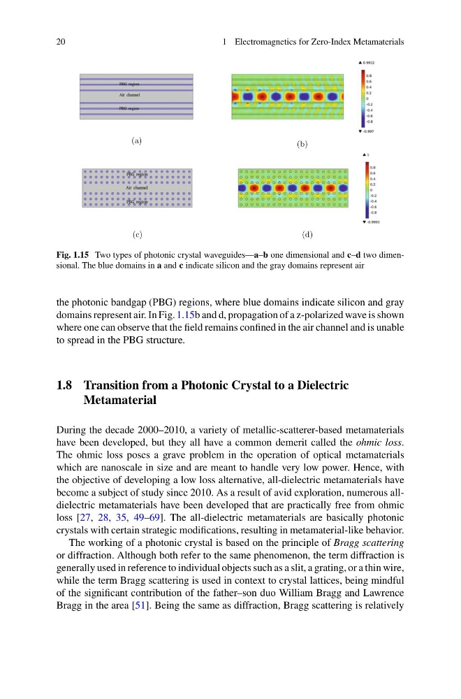
Fig. 1.15 Two types of photonic crystal waveguides—a–b one dimensional and c–d two dimensional. The blue domains in a and c indicate silicon and the gray domains represent air
the photonic bandgap (PBG) regions, where blue domains indicate silicon and gray
domains represent air. In Fig. 1.15b and d, propagation of a z-polarized wave is shown
where one can observe that the field remains confined in the air channel and is unable
to spread in the PBG structure.
1.8 Transition from a Photonic Crystal to a Dielectric
Metamaterial
During the decade 2000–2010, a variety of metallic-scatterer-based metamaterials
have been developed, but they all have a common demerit called the ohmic loss.
The ohmic loss poses a grave problem in the operation of optical metamaterials
which are nanoscale in size and are meant to handle very low power. Hence, with
the objective of developing a low loss alternative, all-dielectric metamaterials have
become a subject of study since 2010. As a result of avid exploration, numerous alldielectric metamaterials have been developed that are practically free from ohmic
loss [27, 28, 35, 49–69]. The all-dielectric metamaterials are basically photonic
crystals with certain strategic modifications, resulting in metamaterial-like behavior.
The working of a photonic crystal is based on the principle of Bragg scattering
or diffraction. Although both refer to the same phenomenon, the term diffraction is
generally used in reference to individual objects such as a slit, a grating, or a thin wire,
while the term Bragg scattering is used in context to crystal lattices, being mindful
of the significant contribution of the father–son duo William Bragg and Lawrence
Bragg in the area [51]. Being the same as diffraction, Bragg scattering is relatively
1 Electromagnetics for Zero-Index Metamaterials
(a)
(b)
(c)
(d)
Fig. 1.15 Two types of photonic crystal waveguides—a–b one dimensional and c–d two dimensional. The blue domains in a and c indicate silicon and the gray domains represent air
the photonic bandgap (PBG) regions, where blue domains indicate silicon and gray
domains represent air. In Fig. 1.15b and d, propagation of a z-polarized wave is shown
where one can observe that the field remains confined in the air channel and is unable
to spread in the PBG structure.
1.8 Transition from a Photonic Crystal to a Dielectric
Metamaterial
During the decade 2000–2010, a variety of metallic-scatterer-based metamaterials
have been developed, but they all have a common demerit called the ohmic loss.
The ohmic loss poses a grave problem in the operation of optical metamaterials
which are nanoscale in size and are meant to handle very low power. Hence, with
the objective of developing a low loss alternative, all-dielectric metamaterials have
become a subject of study since 2010. As a result of avid exploration, numerous alldielectric metamaterials have been developed that are practically free from ohmic
loss [27, 28, 35, 49–69]. The all-dielectric metamaterials are basically photonic
crystals with certain strategic modifications, resulting in metamaterial-like behavior.
The working of a photonic crystal is based on the principle of Bragg scattering
or diffraction. Although both refer to the same phenomenon, the term diffraction is
generally used in reference to individual objects such as a slit, a grating, or a thin wire,
while the term Bragg scattering is used in context to crystal lattices, being mindful
of the significant contribution of the father–son duo William Bragg and Lawrence
Bragg in the area [51]. Being the same as diffraction, Bragg scattering is relatively