

inhomogeneities and defect structures in the interiors of specimens at atomic
resolution. In the meantime, identification of isolated impurity atoms is possible;
however, only under the very best circumstances, such as impurity atoms in
graphene layers [10]. This example is depicted in Figure 12.31. In Figure 12.31a,
the darker parts are the empty spaces within the carbon hexagon. The carbon atoms,
with their higher capability for scattering of electrons, are found in the lighter parts
in between the darker spots. For better clarification, this situation is drawn
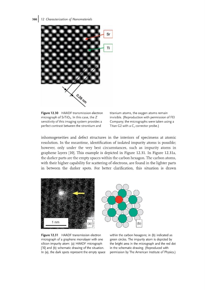
Figure 12.30 HAADF transmission electron
micrograph of SrTiO 3 . In this case, the Z
sensitivity of this imaging system provides a
perfect contrast between the strontium and
titanium atoms, the oxygen atoms remain
invisible. (Reproduction with permission of FEI
Company; the micrographs were taken using a
Titan G2 with a C s corrector probe.)
1 nm
(a)
(b)
Figure 12.31 HAADF transmission electron
micrograph of a graphene monolayer with one
silicon impurity atom: (a) HAADF micrograph
[10] and (b) schematic drawing of the situation.
In (a), the dark spots represent the empty space
within the carbon hexagons; in (b) indicated as
green circles. The impurity atom is depicted by
the bright area in the micrograph and the red dot
in the schematic drawing. (Reproduced with
permission by The American Institute of Physics.)
366j 12 Characterization of Nanomaterials
resolution. In the meantime, identification of isolated impurity atoms is possible;
however, only under the very best circumstances, such as impurity atoms in
graphene layers [10]. This example is depicted in Figure 12.31. In Figure 12.31a,
the darker parts are the empty spaces within the carbon hexagon. The carbon atoms,
with their higher capability for scattering of electrons, are found in the lighter parts
in between the darker spots. For better clarification, this situation is drawn
Figure 12.30 HAADF transmission electron
micrograph of SrTiO 3 . In this case, the Z
sensitivity of this imaging system provides a
perfect contrast between the strontium and
titanium atoms, the oxygen atoms remain
invisible. (Reproduction with permission of FEI
Company; the micrographs were taken using a
Titan G2 with a C s corrector probe.)
1 nm
(a)
(b)
Figure 12.31 HAADF transmission electron
micrograph of a graphene monolayer with one
silicon impurity atom: (a) HAADF micrograph
[10] and (b) schematic drawing of the situation.
In (a), the dark spots represent the empty space
within the carbon hexagons; in (b) indicated as
green circles. The impurity atom is depicted by
the bright area in the micrograph and the red dot
in the schematic drawing. (Reproduced with
permission by The American Institute of Physics.)
366j 12 Characterization of Nanomaterials