

measured this relationship for multiwall nanotubes and Shklyarevskii et al. [8] for
individual graphene layers. In both cases the experiments revealed that, above about
100 mV, the conductivity increased with increasing voltage. For voltages below about
100 mV, the conductance is:
G ¼ G 0 ; V < 100 mV
G ¼ G 0 a þ b V
j j
ð
Þ ; V > 100 mV
ð10:9Þ
where a and b are specimen-dependent factors ranging from 0.25 to a maximum of
1.0. Due to the unavoidable contact resistance, the constant contribution to conductance is usually smaller than G 0 . The function of the conductance is symmetrical
against V ¼ 0 V, according to Eq. (10.9). Due to minor experimental uncertainties,
however, an offset of less than 10 mV is observed. Equation (10.9) leads to a I–V
characteristic such as:
I ¼ VG 0 a þ b V
j j
ð
Þ
ð 10:10Þ
The same relationship was observed for graphene layers, although the relationship to the conductance quantum G 0 is not well defined. The I–V plot for a multiwall
nanotube assuming a ¼ 0.5 and b ¼ 0.25 V
À1 is shown in Figure 10.14, and is
similar to that described for gold nanowires.
Consequently, the electrical conductance of a multiwall nanotube as a function of
the applied voltage has an appearance as shown in Figure 10.15, according to
Poncharal et al. [7].
The I–V characteristic of multiwall carbon nanotubes and individual graphene
layers is entirely different from that of single-wall nanotubes. Likewise, in the case of
single-wall nanotubes, above 100 mV the electrical conductivity depends heavily on
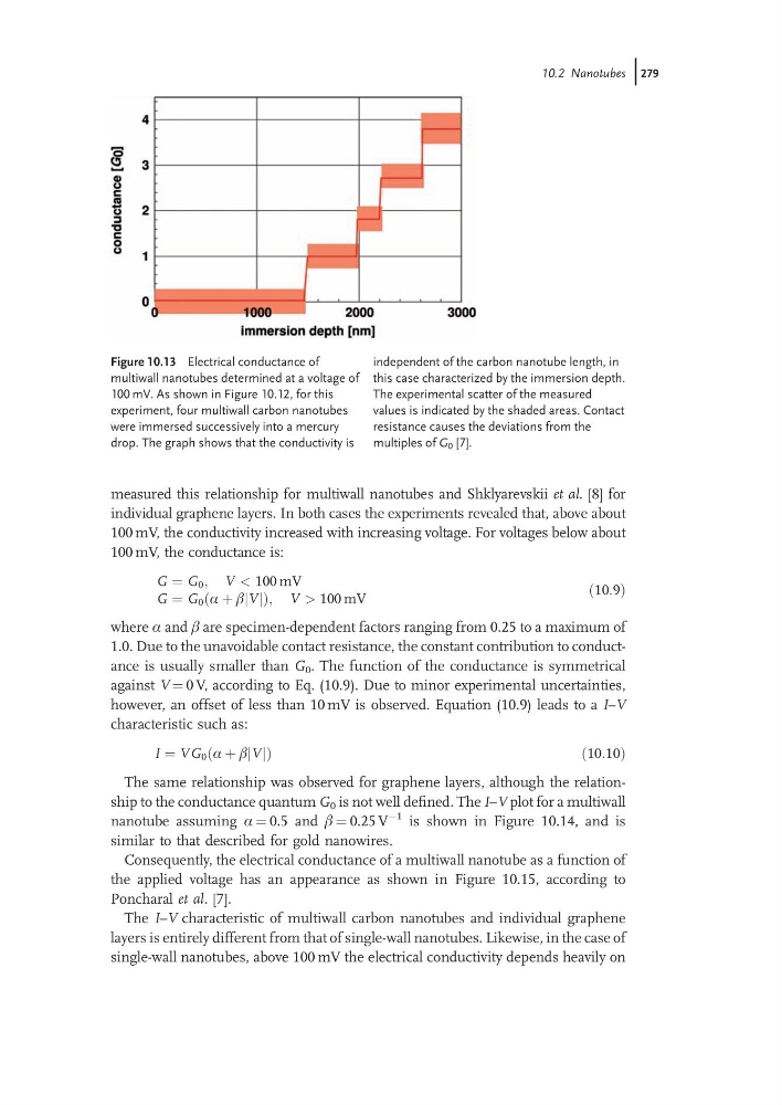
Figure 10.13 Electrical conductance of
multiwall nanotubes determined at a voltage of
100 mV. As shown in Figure 10.12, for this
experiment, four multiwall carbon nanotubes
were immersed successively into a mercury
drop. The graph shows that the conductivity is
independent of the carbon nanotube length, in
this case characterized by the immersion depth.
The experimental scatter of the measured
values is indicated by the shaded areas. Contact
resistance causes the deviations from the
multiples of G 0 [7].
10.2 Nanotubes j279
individual graphene layers. In both cases the experiments revealed that, above about
100 mV, the conductivity increased with increasing voltage. For voltages below about
100 mV, the conductance is:
G ¼ G 0 ; V < 100 mV
G ¼ G 0 a þ b V
j j
ð
Þ ; V > 100 mV
ð10:9Þ
where a and b are specimen-dependent factors ranging from 0.25 to a maximum of
1.0. Due to the unavoidable contact resistance, the constant contribution to conductance is usually smaller than G 0 . The function of the conductance is symmetrical
against V ¼ 0 V, according to Eq. (10.9). Due to minor experimental uncertainties,
however, an offset of less than 10 mV is observed. Equation (10.9) leads to a I–V
characteristic such as:
I ¼ VG 0 a þ b V
j j
ð
Þ
ð 10:10Þ
The same relationship was observed for graphene layers, although the relationship to the conductance quantum G 0 is not well defined. The I–V plot for a multiwall
nanotube assuming a ¼ 0.5 and b ¼ 0.25 V
À1 is shown in Figure 10.14, and is
similar to that described for gold nanowires.
Consequently, the electrical conductance of a multiwall nanotube as a function of
the applied voltage has an appearance as shown in Figure 10.15, according to
Poncharal et al. [7].
The I–V characteristic of multiwall carbon nanotubes and individual graphene
layers is entirely different from that of single-wall nanotubes. Likewise, in the case of
single-wall nanotubes, above 100 mV the electrical conductivity depends heavily on
Figure 10.13 Electrical conductance of
multiwall nanotubes determined at a voltage of
100 mV. As shown in Figure 10.12, for this
experiment, four multiwall carbon nanotubes
were immersed successively into a mercury
drop. The graph shows that the conductivity is
independent of the carbon nanotube length, in
this case characterized by the immersion depth.
The experimental scatter of the measured
values is indicated by the shaded areas. Contact
resistance causes the deviations from the
multiples of G 0 [7].
10.2 Nanotubes j279