

dimensions. The nanotube in Figure 5.40a, which is rather a micro than a nanotube,
has an edge length of more than 1 mm and a wall thickness of approximately 200 nm.
The nanotube shown in Figure 5.40b is entirely different, having an edge length of
approximately 200 nm and a wall thickness of less than 50 nm. When examining
Figure 5.40b in detail, it can be seen that this nanotube, like a whisker, may have
grown as a spiral.
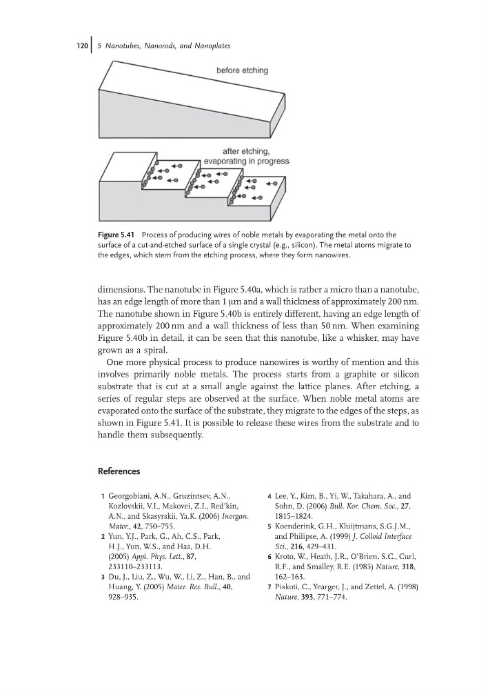
One more physical process to produce nanowires is worthy of mention and this
involves primarily noble metals. The process starts from a graphite or silicon
substrate that is cut at a small angle against the lattice planes. After etching, a
series of regular steps are observed at the surface. When noble metal atoms are
evaporated onto the surface of the substrate, they migrate to the edges of the steps, as
shown in Figure 5.41. It is possible to release these wires from the substrate and to
handle them subsequently.
References
1 Georgobiani, A.N., Gruzintsev, A.N.,
Kozlovskii, V.I., Makovei, Z.I., Red’kin,
A.N., and Skasyrskii, Ya.K. (2006) Inorgan.
Mater., 42, 750–755.
2 Yun, Y.J., Park, G., Ah, C.S., Park,
H.J., Yun, W.S., and Haa, D.H.
(2005) Appl. Phys. Lett., 87,
233110–233113.
3 Du, J., Liu, Z., Wu, W., Li, Z., Han, B., and
Huang, Y. (2005) Mater. Res. Bull., 40,
928–935.
4 Lee, Y., Kim, B., Yi, W., Takahara, A., and
Sohn, D. (2006) Bull. Kor. Chem. Soc., 27,
1815–1824.
5 Koenderink, G.H., Kluijtmans, S.G.J.M.,
and Philipse, A. (1999) J. Colloid Interface
Sci., 216, 429–431.
6 Kroto, W., Heath, J.R., O’Brien, S.C., Curl,
R.F., and Smalley, R.E. (1985) Nature, 318,
162–163.
7 Piskoti, C., Yearger, J., and Zettel, A. (1998)
Nature, 393, 771–774.
Figure 5.41 Process of producing wires of noble metals by evaporating the metal onto the
surface of a cut-and-etched surface of a single crystal (e.g., silicon). The metal atoms migrate to
the edges, which stem from the etching process, where they form nanowires.
120j 5 Nanotubes, Nanorods, and Nanoplates
has an edge length of more than 1 mm and a wall thickness of approximately 200 nm.
The nanotube shown in Figure 5.40b is entirely different, having an edge length of
approximately 200 nm and a wall thickness of less than 50 nm. When examining
Figure 5.40b in detail, it can be seen that this nanotube, like a whisker, may have
grown as a spiral.
One more physical process to produce nanowires is worthy of mention and this
involves primarily noble metals. The process starts from a graphite or silicon
substrate that is cut at a small angle against the lattice planes. After etching, a
series of regular steps are observed at the surface. When noble metal atoms are
evaporated onto the surface of the substrate, they migrate to the edges of the steps, as
shown in Figure 5.41. It is possible to release these wires from the substrate and to
handle them subsequently.
References
1 Georgobiani, A.N., Gruzintsev, A.N.,
Kozlovskii, V.I., Makovei, Z.I., Red’kin,
A.N., and Skasyrskii, Ya.K. (2006) Inorgan.
Mater., 42, 750–755.
2 Yun, Y.J., Park, G., Ah, C.S., Park,
H.J., Yun, W.S., and Haa, D.H.
(2005) Appl. Phys. Lett., 87,
233110–233113.
3 Du, J., Liu, Z., Wu, W., Li, Z., Han, B., and
Huang, Y. (2005) Mater. Res. Bull., 40,
928–935.
4 Lee, Y., Kim, B., Yi, W., Takahara, A., and
Sohn, D. (2006) Bull. Kor. Chem. Soc., 27,
1815–1824.
5 Koenderink, G.H., Kluijtmans, S.G.J.M.,
and Philipse, A. (1999) J. Colloid Interface
Sci., 216, 429–431.
6 Kroto, W., Heath, J.R., O’Brien, S.C., Curl,
R.F., and Smalley, R.E. (1985) Nature, 318,
162–163.
7 Piskoti, C., Yearger, J., and Zettel, A. (1998)
Nature, 393, 771–774.
Figure 5.41 Process of producing wires of noble metals by evaporating the metal onto the
surface of a cut-and-etched surface of a single crystal (e.g., silicon). The metal atoms migrate to
the edges, which stem from the etching process, where they form nanowires.
120j 5 Nanotubes, Nanorods, and Nanoplates