

where the emission increases exponentially with the applied voltage, the emission
showed fluctuations of 50% and more. However, at higher voltages, characterized by
a reduced dependency of the emission on the applied voltage, the emission was
stable for hours (i.e., over a time range that would be applicable for technical
devices).
Electron field emission is of major economic importance in terms of field
emission displays. Compared to tungsten tips, carbon nanotubes have the advantage
of a higher stability of the emission and a better oxidation resistance. This is because,
during field emission, the tungsten cathode tips become very hot, which in turn
causes distortion of the tip geometry and, on occasion, even local melting. Both
events lead not only to deformation, but also to a reduction in the electrical field at
the tip, which is required for emission. Additionally, in contrast to carbon nanotubes, the resistivity of metals increases with temperature and this leads to higher
ohmic losses, which results in even further increases in temperature. This feedback
cycle may cause the tungsten emission tips to be destroyed. Since it is unavoidable
that some residual oxygen will be present in the vacuum of a field emission device,
the heated tungsten cathode oxidizes and this results in a further-reduced field
emission.
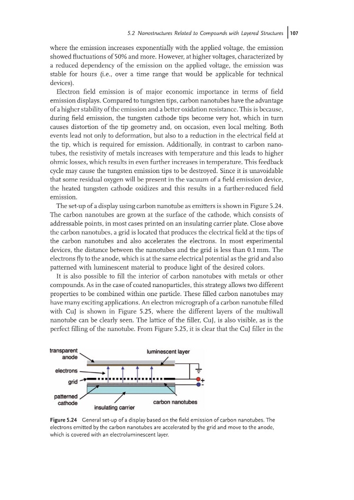
The set-up of a display using carbon nanotube as emitters is shown in Figure 5.24.
The carbon nanotubes are grown at the surface of the cathode, which consists of
addressable points, in most cases printed on an insulating carrier plate. Close above
the carbon nanotubes, a grid is located that produces the electrical field at the tips of
the carbon nanotubes and also accelerates the electrons. In most experimental
devices, the distance between the nanotubes and the grid is less than 0.1 mm. The
electrons fly to the anode, which is at the same electrical potential as the grid and also
patterned with luminescent material to produce light of the desired colors.
It is also possible to fill the interior of carbon nanotubes with metals or other
compounds. As in the case of coated nanoparticles, this strategy allows two different
properties to be combined within one particle. These filled carbon nanotubes may
have many exciting applications. An electron micrograph of a carbon nanotube filled
with CuJ is shown in Figure 5.25, where the different layers of the multiwall
nanotube can be clearly seen. The lattice of the filler, CuJ, is also visible, as is the
perfect filling of the nanotube. From Figure 5.25, it is clear that the CuJ filler in the
Figure 5.24 General set-up of a display based on the field emission of carbon nanotubes. The
electrons emitted by the carbon nanotubes are accelerated by the grid and move to the anode,
which is covered with an electroluminescent layer.
5.2 Nanostructures Related to Compounds with Layered Structures j107
showed fluctuations of 50% and more. However, at higher voltages, characterized by
a reduced dependency of the emission on the applied voltage, the emission was
stable for hours (i.e., over a time range that would be applicable for technical
devices).
Electron field emission is of major economic importance in terms of field
emission displays. Compared to tungsten tips, carbon nanotubes have the advantage
of a higher stability of the emission and a better oxidation resistance. This is because,
during field emission, the tungsten cathode tips become very hot, which in turn
causes distortion of the tip geometry and, on occasion, even local melting. Both
events lead not only to deformation, but also to a reduction in the electrical field at
the tip, which is required for emission. Additionally, in contrast to carbon nanotubes, the resistivity of metals increases with temperature and this leads to higher
ohmic losses, which results in even further increases in temperature. This feedback
cycle may cause the tungsten emission tips to be destroyed. Since it is unavoidable
that some residual oxygen will be present in the vacuum of a field emission device,
the heated tungsten cathode oxidizes and this results in a further-reduced field
emission.
The set-up of a display using carbon nanotube as emitters is shown in Figure 5.24.
The carbon nanotubes are grown at the surface of the cathode, which consists of
addressable points, in most cases printed on an insulating carrier plate. Close above
the carbon nanotubes, a grid is located that produces the electrical field at the tips of
the carbon nanotubes and also accelerates the electrons. In most experimental
devices, the distance between the nanotubes and the grid is less than 0.1 mm. The
electrons fly to the anode, which is at the same electrical potential as the grid and also
patterned with luminescent material to produce light of the desired colors.
It is also possible to fill the interior of carbon nanotubes with metals or other
compounds. As in the case of coated nanoparticles, this strategy allows two different
properties to be combined within one particle. These filled carbon nanotubes may
have many exciting applications. An electron micrograph of a carbon nanotube filled
with CuJ is shown in Figure 5.25, where the different layers of the multiwall
nanotube can be clearly seen. The lattice of the filler, CuJ, is also visible, as is the
perfect filling of the nanotube. From Figure 5.25, it is clear that the CuJ filler in the
Figure 5.24 General set-up of a display based on the field emission of carbon nanotubes. The
electrons emitted by the carbon nanotubes are accelerated by the grid and move to the anode,
which is covered with an electroluminescent layer.
5.2 Nanostructures Related to Compounds with Layered Structures j107