

126
7 Non-conventional Detection Techniques
V a
d
R
V t
n
p
Gold
film
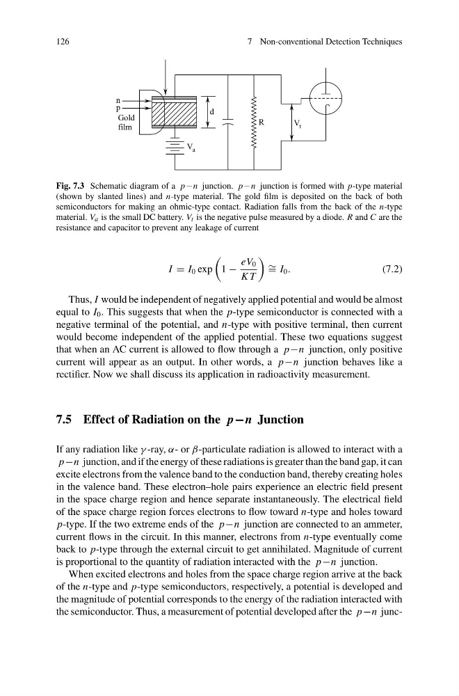
Fig. 7.3 Schematic diagram of a p−n junction. p−n junction is formed with p-type material
(shown by slanted lines) and n-type material. The gold film is deposited on the back of both
semiconductors for making an ohmic-type contact. Radiation falls from the back of the n-type
material. V a is the small DC battery. V t is the negative pulse measured by a diode. R and C are the
resistance and capacitor to prevent any leakage of current
I = I 0 exp
1 −
eV 0
K T
∼ = I 0 .
(7.2)
Thus, I would be independent of negatively applied potential and would be almost
equal to I 0 . This suggests that when the p-type semiconductor is connected with a
negative terminal of the potential, and n-type with positive terminal, then current
would become independent of the applied potential. These two equations suggest
that when an AC current is allowed to flow through a p−n junction, only positive
current will appear as an output. In other words, a p−n junction behaves like a
rectifier. Now we shall discuss its application in radioactivity measurement.
7.5 Effect of Radiation on the p−n Junction
If any radiation like γ -ray, α- or β-particulate radiation is allowed to interact with a
p−n junction, and if the energy of these radiations is greater than the band gap, it can
excite electrons from the valence band to the conduction band, thereby creating holes
in the valence band. These electron–hole pairs experience an electric field present
in the space charge region and hence separate instantaneously. The electrical field
of the space charge region forces electrons to flow toward n-type and holes toward
p-type. If the two extreme ends of the p−n junction are connected to an ammeter,
current flows in the circuit. In this manner, electrons from n-type eventually come
back to p-type through the external circuit to get annihilated. Magnitude of current
is proportional to the quantity of radiation interacted with the p−n junction.
When excited electrons and holes from the space charge region arrive at the back
of the n-type and p-type semiconductors, respectively, a potential is developed and
the magnitude of potential corresponds to the energy of the radiation interacted with
the semiconductor. Thus, a measurement of potential developed after the p−n junc-
7 Non-conventional Detection Techniques
V a
d
R
V t
n
p
Gold
film
Fig. 7.3 Schematic diagram of a p−n junction. p−n junction is formed with p-type material
(shown by slanted lines) and n-type material. The gold film is deposited on the back of both
semiconductors for making an ohmic-type contact. Radiation falls from the back of the n-type
material. V a is the small DC battery. V t is the negative pulse measured by a diode. R and C are the
resistance and capacitor to prevent any leakage of current
I = I 0 exp
1 −
eV 0
K T
∼ = I 0 .
(7.2)
Thus, I would be independent of negatively applied potential and would be almost
equal to I 0 . This suggests that when the p-type semiconductor is connected with a
negative terminal of the potential, and n-type with positive terminal, then current
would become independent of the applied potential. These two equations suggest
that when an AC current is allowed to flow through a p−n junction, only positive
current will appear as an output. In other words, a p−n junction behaves like a
rectifier. Now we shall discuss its application in radioactivity measurement.
7.5 Effect of Radiation on the p−n Junction
If any radiation like γ -ray, α- or β-particulate radiation is allowed to interact with a
p−n junction, and if the energy of these radiations is greater than the band gap, it can
excite electrons from the valence band to the conduction band, thereby creating holes
in the valence band. These electron–hole pairs experience an electric field present
in the space charge region and hence separate instantaneously. The electrical field
of the space charge region forces electrons to flow toward n-type and holes toward
p-type. If the two extreme ends of the p−n junction are connected to an ammeter,
current flows in the circuit. In this manner, electrons from n-type eventually come
back to p-type through the external circuit to get annihilated. Magnitude of current
is proportional to the quantity of radiation interacted with the p−n junction.
When excited electrons and holes from the space charge region arrive at the back
of the n-type and p-type semiconductors, respectively, a potential is developed and
the magnitude of potential corresponds to the energy of the radiation interacted with
the semiconductor. Thus, a measurement of potential developed after the p−n junc-