

7.4 Formation of p : p Junction
125
w w
C
N
+
P
h +
e
p-type
a
–
b
c
P
n-type
e
e
A
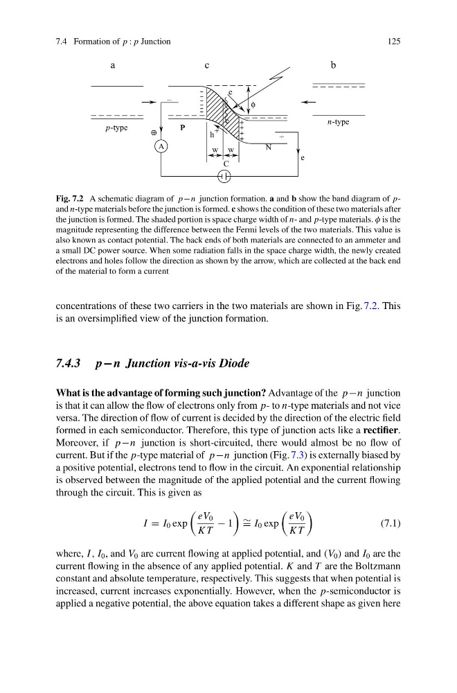
Fig. 7.2 A schematic diagram of p−n junction formation. a and b show the band diagram of pand n-type materials before the junction is formed. c shows the condition of these two materials after
the junction is formed. The shaded portion is space charge width of n- and p-type materials. φ is the
magnitude representing the difference between the Fermi levels of the two materials. This value is
also known as contact potential. The back ends of both materials are connected to an ammeter and
a small DC power source. When some radiation falls in the space charge width, the newly created
electrons and holes follow the direction as shown by the arrow, which are collected at the back end
of the material to form a current
concentrations of these two carriers in the two materials are shown in Fig. 7.2. This
is an oversimplified view of the junction formation.
7.4.3 p−n Junction vis-a-vis Diode
What is the advantage of forming such junction? Advantage of the p−n junction
is that it can allow the flow of electrons only from p- to n-type materials and not vice
versa. The direction of flow of current is decided by the direction of the electric field
formed in each semiconductor. Therefore, this type of junction acts like a rectifier.
Moreover, if p−n junction is short-circuited, there would almost be no flow of
current. But if the p-type material of p−n junction (Fig. 7.3) is externally biased by
a positive potential, electrons tend to flow in the circuit. An exponential relationship
is observed between the magnitude of the applied potential and the current flowing
through the circuit. This is given as
I = I 0 exp
eV 0
K T
− 1
∼ = I 0 exp
eV 0
K T
(7.1)
where, I , I 0 , and V 0 are current flowing at applied potential, and (V 0 ) and I 0 are the
current flowing in the absence of any applied potential. K and T are the Boltzmann
constant and absolute temperature, respectively. This suggests that when potential is
increased, current increases exponentially. However, when the p-semiconductor is
applied a negative potential, the above equation takes a different shape as given here
125
w w
C
N
+
P
h +
e
p-type
a
–
b
c
P
n-type
e
e
A
Fig. 7.2 A schematic diagram of p−n junction formation. a and b show the band diagram of pand n-type materials before the junction is formed. c shows the condition of these two materials after
the junction is formed. The shaded portion is space charge width of n- and p-type materials. φ is the
magnitude representing the difference between the Fermi levels of the two materials. This value is
also known as contact potential. The back ends of both materials are connected to an ammeter and
a small DC power source. When some radiation falls in the space charge width, the newly created
electrons and holes follow the direction as shown by the arrow, which are collected at the back end
of the material to form a current
concentrations of these two carriers in the two materials are shown in Fig. 7.2. This
is an oversimplified view of the junction formation.
7.4.3 p−n Junction vis-a-vis Diode
What is the advantage of forming such junction? Advantage of the p−n junction
is that it can allow the flow of electrons only from p- to n-type materials and not vice
versa. The direction of flow of current is decided by the direction of the electric field
formed in each semiconductor. Therefore, this type of junction acts like a rectifier.
Moreover, if p−n junction is short-circuited, there would almost be no flow of
current. But if the p-type material of p−n junction (Fig. 7.3) is externally biased by
a positive potential, electrons tend to flow in the circuit. An exponential relationship
is observed between the magnitude of the applied potential and the current flowing
through the circuit. This is given as
I = I 0 exp
eV 0
K T
− 1
∼ = I 0 exp
eV 0
K T
(7.1)
where, I , I 0 , and V 0 are current flowing at applied potential, and (V 0 ) and I 0 are the
current flowing in the absence of any applied potential. K and T are the Boltzmann
constant and absolute temperature, respectively. This suggests that when potential is
increased, current increases exponentially. However, when the p-semiconductor is
applied a negative potential, the above equation takes a different shape as given here