

90
Y. Li et al.
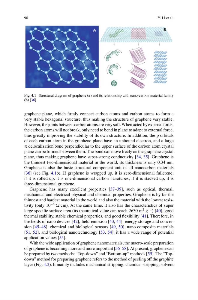
Fig. 4.1 Structural diagram of graphene (a) and its relationship with nano-carbon material family
(b) [36]
graphene plane, which firmly connect carbon atoms and carbon atoms to form a
very stable hexagonal structure, thus making the structure of graphene very stable.
However, the joints between carbon atoms are very soft. When acted by external force,
the carbon atoms will not break, only need to bend in plane to adapt to external force,
thus greatly improving the stability of its own structure. In addition, the p orbitals
of each carbon atom in the graphene plane have an unbound electron, and a large
π delocalization bond perpendicular to the upper surface of the carbon atom crystal
plane can be formed between them. The bond can move freely on the graphene crystal
plane, thus making graphene have super-strong conductivity [34, 35]. Graphene is
the thinnest two-dimensional material in the world, its thickness is only 0.34 nm.
Graphene is also the basic structural component unit of all nanocarbon materials
[36] (see Fig. 4.1b). If graphene is wrapped up, it is zero-dimensional fullerene;
if it is rolled up, it is one-dimensional carbon nanotubes; if it is stacked up, it is
three-dimensional graphene.
Graphene has many excellent properties [37–39], such as optical, thermal,
mechanical and electrical physical and chemical properties. Graphene is by far the
thinnest and hardest material in the world and also the material with the lowest resistivity (only 10
−6
·cm). At the same time, it also has the characteristics of super
large specific surface area (its theoretical value can reach 2630 m
2 g
−1 ) [40], good
thermal stability, stable chemical properties, and good flexibility [41]. Therefore, in
the fields of nano devices [42], field emission [43, 44], energy storage and conversion [45–48], chemical and biological sensors [49, 50], nano composite materials
[51, 52], and biological nanotechnology [53, 54], it has a wide range of potential
application values [55].
With the wide application of graphene nanomaterials, the macro-scale preparation
of graphene is becoming more and more important [56–58]. At present, graphene can
be prepared by two methods: “Top-down” and “Bottom-up” methods [55]. The “Topdown” method for preparing graphene refers to the method of peeling off the graphite
layer (Fig. 4.2). It mainly includes mechanical stripping, chemical stripping, solvent
Y. Li et al.
Fig. 4.1 Structural diagram of graphene (a) and its relationship with nano-carbon material family
(b) [36]
graphene plane, which firmly connect carbon atoms and carbon atoms to form a
very stable hexagonal structure, thus making the structure of graphene very stable.
However, the joints between carbon atoms are very soft. When acted by external force,
the carbon atoms will not break, only need to bend in plane to adapt to external force,
thus greatly improving the stability of its own structure. In addition, the p orbitals
of each carbon atom in the graphene plane have an unbound electron, and a large
π delocalization bond perpendicular to the upper surface of the carbon atom crystal
plane can be formed between them. The bond can move freely on the graphene crystal
plane, thus making graphene have super-strong conductivity [34, 35]. Graphene is
the thinnest two-dimensional material in the world, its thickness is only 0.34 nm.
Graphene is also the basic structural component unit of all nanocarbon materials
[36] (see Fig. 4.1b). If graphene is wrapped up, it is zero-dimensional fullerene;
if it is rolled up, it is one-dimensional carbon nanotubes; if it is stacked up, it is
three-dimensional graphene.
Graphene has many excellent properties [37–39], such as optical, thermal,
mechanical and electrical physical and chemical properties. Graphene is by far the
thinnest and hardest material in the world and also the material with the lowest resistivity (only 10
−6
·cm). At the same time, it also has the characteristics of super
large specific surface area (its theoretical value can reach 2630 m
2 g
−1 ) [40], good
thermal stability, stable chemical properties, and good flexibility [41]. Therefore, in
the fields of nano devices [42], field emission [43, 44], energy storage and conversion [45–48], chemical and biological sensors [49, 50], nano composite materials
[51, 52], and biological nanotechnology [53, 54], it has a wide range of potential
application values [55].
With the wide application of graphene nanomaterials, the macro-scale preparation
of graphene is becoming more and more important [56–58]. At present, graphene can
be prepared by two methods: “Top-down” and “Bottom-up” methods [55]. The “Topdown” method for preparing graphene refers to the method of peeling off the graphite
layer (Fig. 4.2). It mainly includes mechanical stripping, chemical stripping, solvent