

494
Y. Yoshida
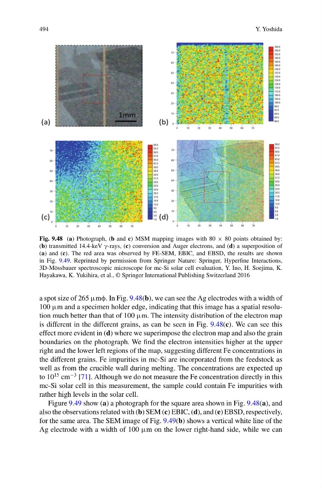
Fig. 9.48 (a) Photograph, (b and c) MSM mapping images with 80 × 80 points obtained by:
(b) transmitted 14.4-keV γ-rays, (c) conversion and Auger electrons, and (d) a superposition of
(a) and (c). The red area was observed by FE-SEM, EBIC, and EBSD, the results are shown
in Fig. 9.49. Reprinted by permission from Springer Nature: Springer, Hyperfine Interactions,
3D-Mössbauer spectroscopic microscope for mc-Si solar cell evaluation, Y. Ino, H. Soejima, K.
Hayakawa, K. Yukihira, et al., © Springer International Publishing Switzerland 2016
a spot size of 265 μmφ. In Fig. 9.48(b), we can see the Ag electrodes with a width of
100 μm and a specimen holder edge, indicating that this image has a spatial resolution much better than that of 100 μm. The intensity distribution of the electron map
is different in the different grains, as can be seen in Fig. 9.48(c). We can see this
effect more evident in (d) where we superimpose the electron map and also the grain
boundaries on the photograph. We find the electron intensities higher at the upper
right and the lower left regions of the map, suggesting different Fe concentrations in
the different grains. Fe impurities in mc-Si are incorporated from the feedstock as
well as from the crucible wall during melting. The concentrations are expected up
to 10
15 cm
−3 [71]. Although we do not measure the Fe concentration directly in this
mc-Si solar cell in this measurement, the sample could contain Fe impurities with
rather high levels in the solar cell.
Figure 9.49 show (a) a photograph for the square area shown in Fig. 9.48(a), and
also the observations related with (b) SEM (c) EBIC, (d), and (e) EBSD, respectively,
for the same area. The SEM image of Fig. 9.49(b) shows a vertical white line of the
Ag electrode with a width of 100 μm on the lower right-hand side, while we can
Y. Yoshida
Fig. 9.48 (a) Photograph, (b and c) MSM mapping images with 80 × 80 points obtained by:
(b) transmitted 14.4-keV γ-rays, (c) conversion and Auger electrons, and (d) a superposition of
(a) and (c). The red area was observed by FE-SEM, EBIC, and EBSD, the results are shown
in Fig. 9.49. Reprinted by permission from Springer Nature: Springer, Hyperfine Interactions,
3D-Mössbauer spectroscopic microscope for mc-Si solar cell evaluation, Y. Ino, H. Soejima, K.
Hayakawa, K. Yukihira, et al., © Springer International Publishing Switzerland 2016
a spot size of 265 μmφ. In Fig. 9.48(b), we can see the Ag electrodes with a width of
100 μm and a specimen holder edge, indicating that this image has a spatial resolution much better than that of 100 μm. The intensity distribution of the electron map
is different in the different grains, as can be seen in Fig. 9.48(c). We can see this
effect more evident in (d) where we superimpose the electron map and also the grain
boundaries on the photograph. We find the electron intensities higher at the upper
right and the lower left regions of the map, suggesting different Fe concentrations in
the different grains. Fe impurities in mc-Si are incorporated from the feedstock as
well as from the crucible wall during melting. The concentrations are expected up
to 10
15 cm
−3 [71]. Although we do not measure the Fe concentration directly in this
mc-Si solar cell in this measurement, the sample could contain Fe impurities with
rather high levels in the solar cell.
Figure 9.49 show (a) a photograph for the square area shown in Fig. 9.48(a), and
also the observations related with (b) SEM (c) EBIC, (d), and (e) EBSD, respectively,
for the same area. The SEM image of Fig. 9.49(b) shows a vertical white line of the
Ag electrode with a width of 100 μm on the lower right-hand side, while we can